

Pad layout structure of a driver IC chip
Patent Information
- Authority / Receiving Office
- US · United States
- Current Assignee / Owner
- SILICON WORKS CO LTD
- Publication Date
- 2011-04-21
Smart Images
Figure 1 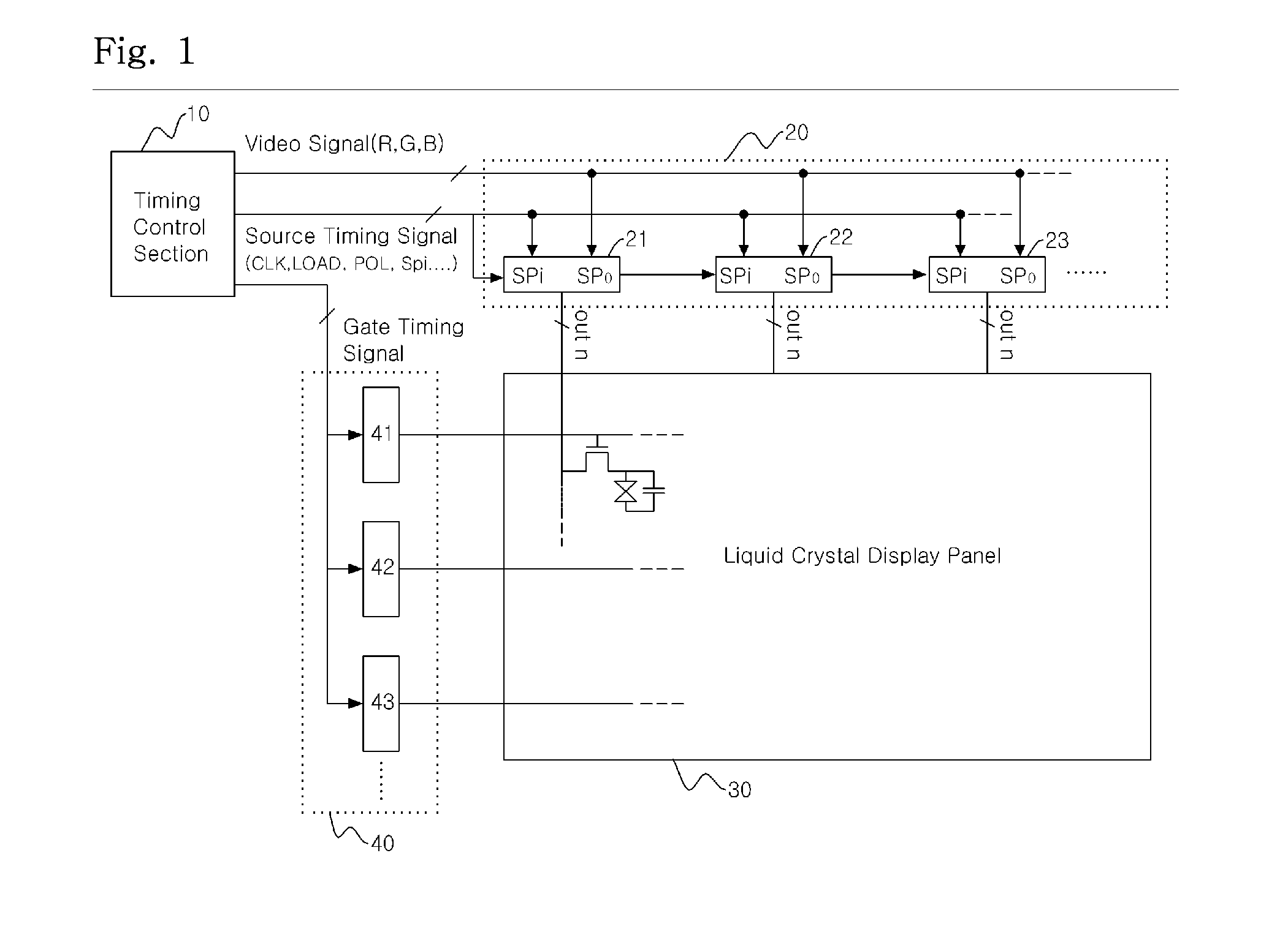
Figure 2 
Figure 3
Abstract
Description
BACKGROUND OF THE INVENTION
[0001] 1. Field of the Invention
[0002] The present invention relates to a pad layout structure of a driver IC (integrated circuit) chip in a liquid crystal display, and more particularly, to a pad layout structure of a driver IC chip in which, when mounting a driver IC chip to a liquid crystal display panel in a chip-on-glass (COG) type, power pads of the driver IC chip are located at the corners of the driver IC chip in all four directions so that the adhesion between the driver IC chip and the liquid crystal display panel can be enhanced.
[0003] 2. Description of the Related Art
[0004] A liquid crystal display (LCD) indicates a device in which image data is displayed by passing light rays through liquid crystal based on the fact that the alignment of liquid crystal molecules is changed depending upon an applied voltage. Among LCDs, a thin film transistor (TFT) LCD, which is manufactured using technology for manufacturing a silicon integrated circuit, is most ...