Thin film transistor with self-aligned intra-gate electrode

a thin film transistor and intra-gate electrode technology, applied in the field of thin film transistors, can solve the problems of low response speed, photo-misalignment problem, and restricted application, and achieve the effect of reducing the problem of photo-misalignmen

Inactive Publication Date: 2006-03-07
INNOLUX CORP
View PDF1 Cites 68 Cited by
  • Summary
  • Abstract
  • Description
  • Claims
  • Application Information

AI Technical Summary

Benefits of technology

[0007]It is an aspect of the present invention to provide a thin film transistor for use in an active matrix liquid crystal display (AM-LCD) so as to minimize the problem of photo-misalignment.
[0008]It is another aspect of the present invention to provide a thin film transistor capable of providing associated functions of LDD regions so as to provide good image characteristics of the active matrix liquid crystal display (AM-LCD).
[0009]It is another aspect of the present invention to provide a thin film transistor formed by self-align process, in which the gate characteristic length of the thin film transistor can be shortened according to the features of the components, thereby increasing aperture ratio of the pixel and reducing surface reflection of the polysilicon layer.

Problems solved by technology

However, since such LCDs have disadvantages of insufficient brightness, narrow viewing angle and low response speed, their applications are restricted.
For example, a photo-misalignment problem occurs because at least two masks and at least two ion-implanting steps are required for forming the LDD regions 24.
Such photo-misalignment problem impairs electrical properties of the TFT and thus image quality of the liquid crystal display.

Method used


Image

  • Thin film transistor with self-aligned intra-gate electrode
  • Thin film transistor with self-aligned intra-gate electrode
  • Thin film transistor with self-aligned intra-gate electrode

Examples


first embodiment

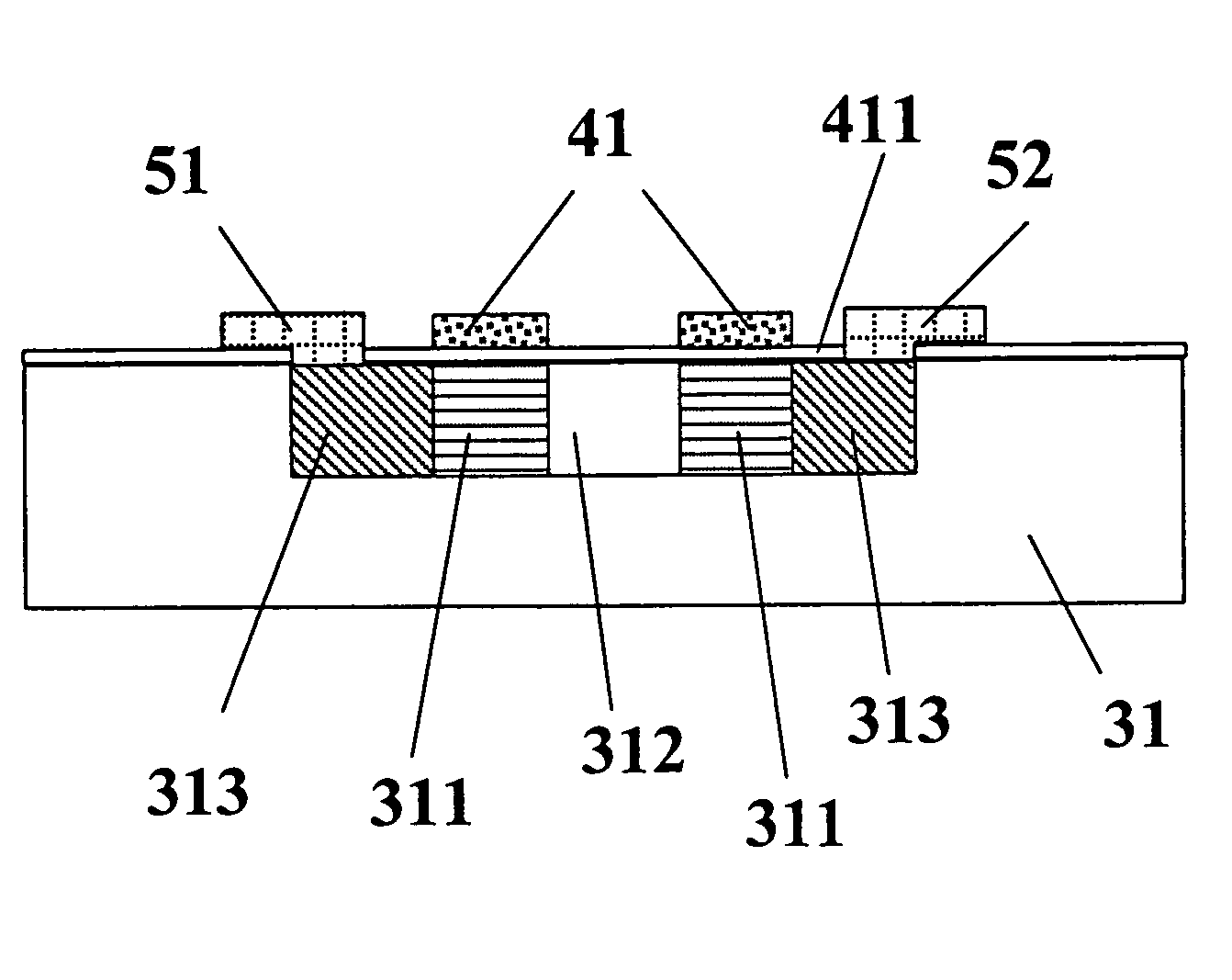
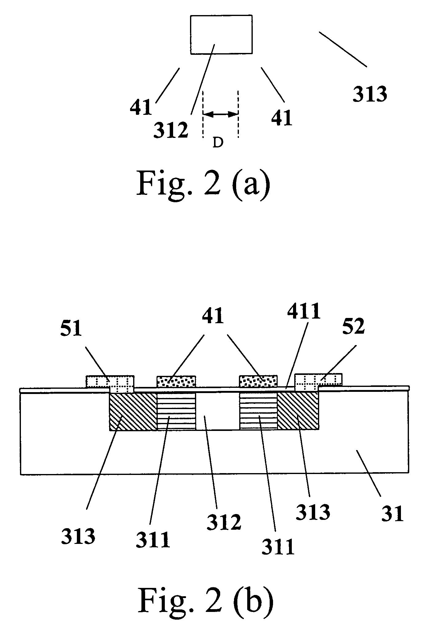
[0029]FIGS. 2(a) and 2(b) are top view and cross-sectional view illustrating a thin film transistor for use in an active matrix liquid crystal display according to the present invention, respectively. The thin film transistor of the present invention comprises a substrate 31. In the substrate 31, there is provided a plurality of intrinsic regions 311, at least one first doped region 312 (which can be n-doped regions) and two second doped regions 313. The first doped region 312 is disposed between the intrinsic regions 311. The intrinsic regions 311 are linked together to form a connection structure via the first doped region 312. The two second doped regions 313 are disposed at both ends of the connection structure, respectively. Furthermore, this thin film transistor further comprises a source region 51 and a drain region 52, which are coupled to the two second doped regions 313 disposed at both ends of the connection structure, respectively. This thin film transistor further compr...

second embodiment

[0030]FIGS. 3(a) and 3(b) are schematic views illustrating a thin film transistor according to the present invention. In FIG. 3(a), the relative locations of the intrinsic regions 311, the first doped region 312 and the second doped regions 313 are shown. The intrinsic regions 311, the first doped region 312 and the second doped regions 313 are arranged in an inverse L-shaped configuration. In other words, the first doped region 312 comprises two portions in vertical arrangement to each other. The intrinsic regions 311 are linked together to form a connection structure via the first doped region 312. The two second doped regions 313 are disposed at both ends of the connection structure, respectively. Furthermore, this thin film transistor further comprises a source region and a drain region (not shown), which are coupled to the two second doped regions 313 disposed at both ends of the connection structure, respectively. In FIG. 3(b), the gate electrode 41 is arranged in an L-shaped ...

third embodiment

[0031]the present invention can be seen in FIGS. 4(a) and 4(b). In FIG. 4(a), the relative locations of the intrinsic regions 311, the first doped region 312 and the second doped regions 313 are shown. The intrinsic regions 311, the first doped region 312 and the second doped regions 313 are arranged in approximately a U-shaped configuration. In other words, the first doped region 312 is arranged in approximately a U-shaped configuration. The intrinsic regions 311 are linked together to form a connection structure via the first doped region 312. The two second doped regions 313 are disposed at both ends of the connection structure, respectively. Furthermore, this thin film transistor further comprises a source region and a drain region (not shown), which are coupled to the two second doped regions 313 disposed at both ends of the connection structure, respectively. In FIG. 4(b), the gate electrode 41 is arranged in an I-shaped configuration and disposed over the intrinsic regions 31...


PUM


Abstract

A thin film transistor for use in an active matrix liquid crystal display includes a substrate, a source and a drain regions, and at least a gate electrode. The substrate includes therein a plurality of intrinsic regions, at least one first doped region and two second doped regions. The first doped region is disposed between the plurality of intrinsic regions. The plurality of intrinsic regions are linked together to form a connection structure via the first doped region, and the two second doped regions are disposed at both ends of the connection structure, respectively. The source and the drain regions are coupled to the two second doped regions disposed at both ends of the connection structure, respectively. The gate electrode is disposed over the plurality of intrinsic regions, such that the periphery of each of the plurality of intrinsic regions and the periphery of a corresponding gate electrode are substantially aligned with each other.

Description

FIELD OF THE INVENTION[0001]The present invention relates to a thin film transistor for use in an active matrix liquid crystal display (AM-LCD), and more particularly to a thin film transistor with a self-align intra-gate electrode.BACKGROUND OF THE INVENTION[0002]With increasing development, liquid crystal displays (LCDs) are widely used due to their advantages of small size, light weight, low driving voltage, low power consumption and good portability. The liquid crystal molecules of the liquid crystal displays are aligned in response to electrical filed changes, thereby controlling the brightness or darkness of the liquid crystal display.[0003]According the production technologies, liquid crystal displays are typically classified into two major types, i.e. a passive matrix liquid crystal display (PM-LCD) and an active matrix liquid crystal display (AM-LCD). In 1970s, the PM-LCDs have been applied in watches and portable calculators. However, since such LCDs have disadvantages of ...

Claims


Application Information

Patent Timeline
Patent Type & Authority Patents(United States)
IPC IPC(8): H01L29/04H01L29/423H01L29/786
CPCH01L29/42384H01L29/78696H01L29/78675H01L29/78645
Inventor TSAI, YAW-MINGHSIEH, HSIU-CHUNCHANG, SHIH-CHANGHUANG, CHEN-TINGWU, I-WEI
Owner INNOLUX CORP
Why Eureka
Try Eureka