Semiconductor light-emitting apparatus

Active Publication Date: 2011-04-21
PANASONIC CORP
View PDF9 Cites 57 Cited by
  • Summary
  • Abstract
  • Description
  • Claims
  • Application Information

AI Technical Summary

Benefits of technology

[0019]According to the semiconductor light-emitting apparatus having the above structure, in each of the protrusions that compose the light-emitting part, the primary light and the secondary light incident from a base end of each protrusion are repeatedly reflected within the protrusion so that the wavelength thereof are guided, and subsequently the light exits from the top en

Problems solved by technology

However, according to the white LED package described in Patent Citatio

Method used


Image

  • Semiconductor light-emitting apparatus
  • Semiconductor light-emitting apparatus
  • Semiconductor light-emitting apparatus

Examples


Example

Embodiment 1

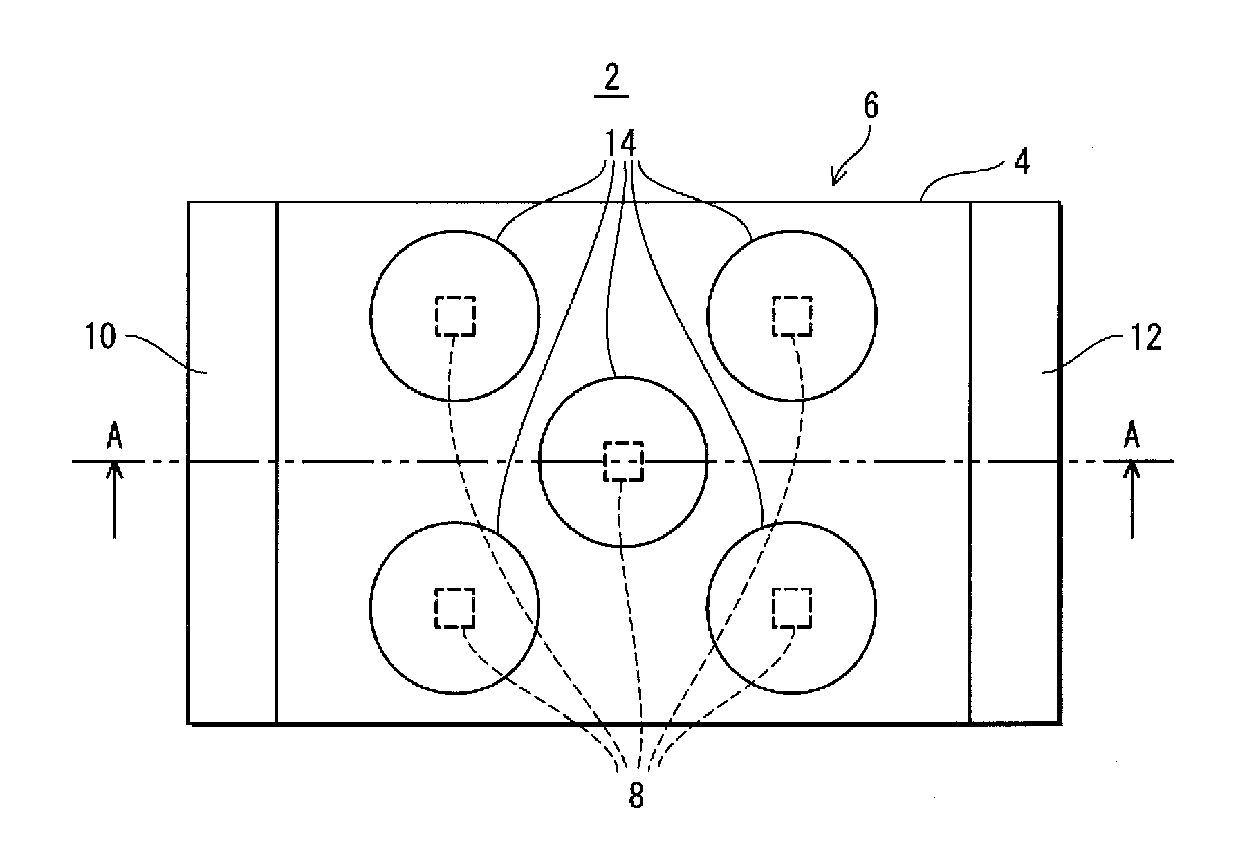
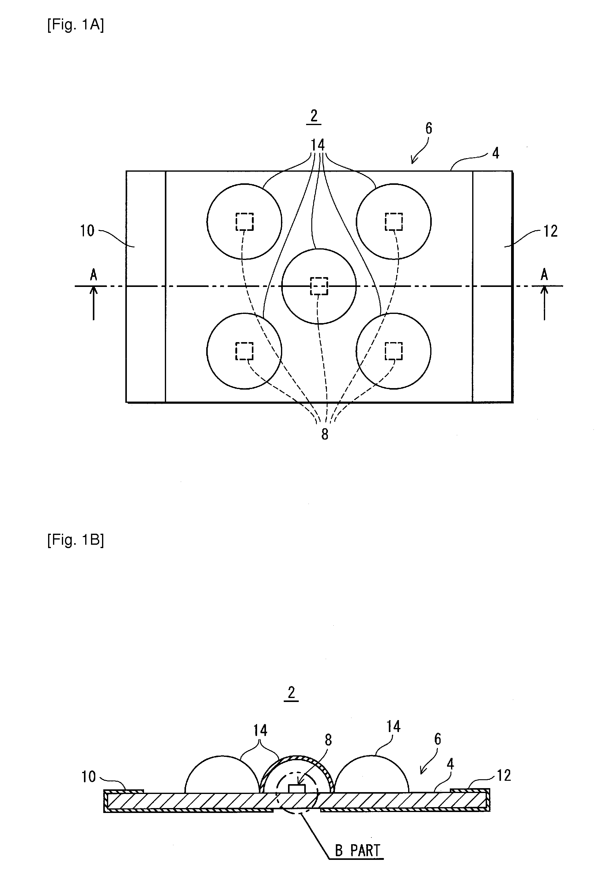
[0048]FIG. 1 schematically shows a surface-mount white LED package 2 (hereinafter, simply referred to as “LED package 2”) as an embodiment of the semiconductor light-emitting apparatus in accordance with the present invention. FIG. 1A is a plan view of the LED package 2. FIG. 1B is a cross section view taken along line A-A of FIG. 1A. Note that scales of constituents in all the drawings including FIG. 1 are not unified.

[0049]The LED package 2 has a printed-wiring board 6 composed of the insulating substrate 4 on which a wiring pattern (unshown in FIG. 1) is printed. The insulating substrate 4 is made of aluminum nitride (AlN) and is a base on which the semi-conductor light-emitting device is mounted. The size of the insulating substrate 4 is 30 [millimeter]*50 [millimeter]*1.5 [millimeter] which are respectively length*width*thickness.

[0050]On the printed-wiring board 6, a plurality of white LEDs 8 (five in this embodiment) are arranged. These white LEDs 8 are connected ...

Example

Embodiment 2

[0104]FIG. 5 is a cross section view schematically showing a surface-mount white LED package 50 (hereinafter, simply referred to as “LED package 50”) in accordance with Embodiment 2 of the present invention.

[0105]The LED package 50 is different from the LED package 2 (FIG. 1) of Embodiment 1, and is composed of one blue LED 52. The phosphor plate 54 of the LED package 50 is made of the same material as the phosphor plate 30 of Embodiment 1. The shape and the like of each light waveguide part 44 are determined from the similar viewpoint, and thus descriptions thereof are omitted here.

[0106]The blue LED 52 is a chip-shaped LED with the pair of p-side and n-side electrodes facing up, and is mounted on the insulating substrate 56. The p-side electrode (unshown) of the blue LED 52 and the anode terminal 58 formed on the insulating substrate 56 are connected with each other via the bonding wire 60. On the other hand, the n-side electrode (unshown) and the cathode terminal 62 f...

Example

Embodiment 3

[0109]FIG. 6 is a cross section view schematically showing a surface-mount white LED package 80 (hereinafter, simply referred to as “LED package 80”) in accordance with Embodiment 3 of the present invention.

[0110]The LED package 80 has a structure basically identical with the LED package 50 (FIG. 5) of Embodiment 2 except for the overall shape of the phosphor plate. Therefore, in FIG. 6, constituents of the LED package 80 common to those of the LED package 50 have the identical reference numbers, and descriptions thereof are omitted.

[0111]The phosphor plate 82 of the LED package 80 is generally dome-shaped (half-sphere). Because of this shape, the LED package 80 can obtain a wider light distribution curve than that of the LED package 50.


PUM


Abstract

A blue LED 18 that is a semiconductor light-emitting device and that emits blue light as primary light having a peak wavelength in a visible region and a phosphor plate 30 that is a wavelength converter and that converts a portion of the blue light emitted from the blue LED 18 into yellow light as secondary light having a longer peak wavelength in the visible region than the peak wavelength and emits the yellow light in combination with a remainder of the blue light left unconverted. The phosphor plate 30 includes (a) a main body 39 extending across a light-emission path of the blue LED 18 and (b) a light-emitting part 42 composed of a plurality of columnar protrusions 44 on a part of the main body 39 in a direction in which the light exits.

Description

TECHNICAL FIELD[0001]The present invention relates to a semiconductor light-emitting apparatus, and in particular to a semiconductor light-emitting apparatus having a semiconductor light-emitting device and a wavelength converter that converts primary light emitted from the light-emitting device to secondary light having a wavelength different from that of the primary light.BACKGROUND ART[0002]In recent years, a white LED package that is one type of a semiconductor light-emitting apparatus is widely used as an alternative to a conventional lighting fixture, such as a fluorescent lamp. It is generally known that a white LED can be achieved by combining a blue LED which is one type of the semiconductor light-emitting device and a yellow phosphor which is a wavelength conversion material. The white LED generates white light as follows. The blue LED emits blue light (primary light) and the blue light excites a yellow phosphor to generate yellow light (secondary light). The blue light th...

Claims


Application Information

Patent Timeline
IPC IPC(8): F21V9/00H01L33/50
CPCH01L33/505H01L33/508H01L2933/0083H01L2933/0091H01L2224/48091H01L2924/00014
Inventor NAGAI, HIDEOUENO, YASUHARU
Owner PANASONIC CORP
Why Eureka
Try Eureka