Semiconductor device and method for manufacturing the same

a technology of semiconductor devices and semiconductors, applied in the direction of semiconductor devices, radiation controlled devices, electrical devices, etc., can solve problems such as leakage defects

Active Publication Date: 2011-04-28
ADVANCED ION BEAM TECHNOLOGY INC
View PDF46 Cites 5 Cited by
  • Summary
  • Abstract
  • Description
  • Claims
  • Application Information

AI Technical Summary

Benefits of technology

[0008]The present invention is directed to a semiconductor device and a method for manufacturing the same, wherein the possib

Problems solved by technology

The carbon-rich regions 160 fabricated by the above-mentioned manufacturing method, however, ma

Method used


Image

  • Semiconductor device and method  for manufacturing the same
  • Semiconductor device and method  for manufacturing the same
  • Semiconductor device and method  for manufacturing the same

Examples


Embodiment Construction

[0018]Reference will now be made in detail to specific embodiments of the present invention that are illustrated in the accompanying drawings. While the invention is described in conjunction with these specific embodiments, it is not intended to limit the invention to these embodiments. In contrast, it is intended to cover alternatives, modifications, and equivalents as may be included within the spirit and scope of the invention as defined by the appended claims. The present invention may be practiced without at least one of these specific details.

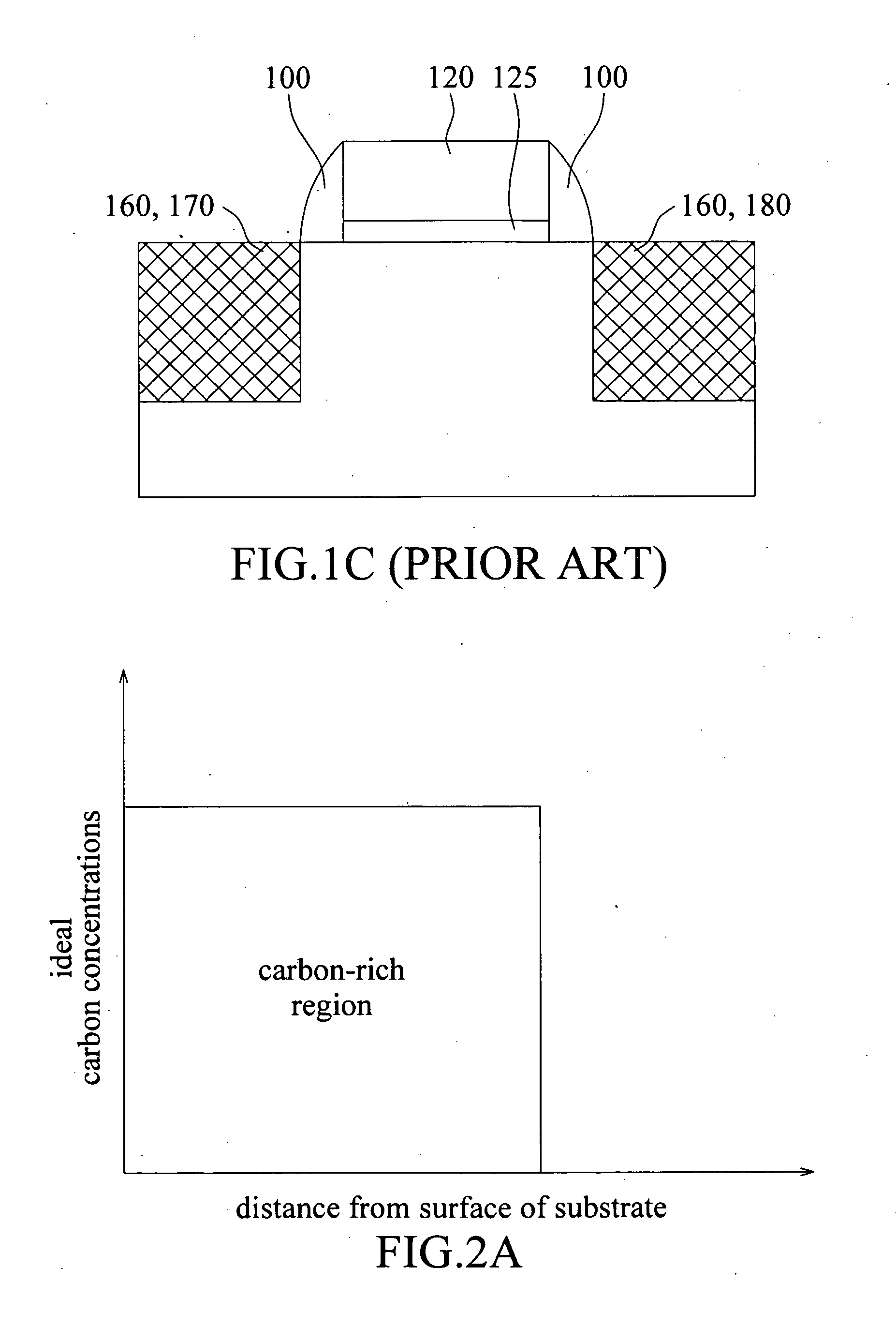
[0019]One embodiment for showing some characteristics of this invention is illustrated in FIG. 2A to FIG. 2D. FIG. 2A shows an ideal carbon-concentration vs. depth (measured from the top surface of a substrate) relation of a carbon-rich region with a specific dose, and FIG. 2B shows a real absolute value of gradient of carbon concentration vs. depth (measured from the top surface of a substrate) relation of a carbon-rich region with a spe...


PUM


Abstract

A semiconductor device has at least two main carbon-rich regions and two additional carbon-rich regions. The main carbon-rich regions are separately located in a substrate so that a channel region is located between them. The additional carbon-rich regions are respectively located underneath the main carbon-rich regions. The carbon concentrations is higher in the main carbon-rich regions and lower in the additional carbon-rich regions, and optionally, the absolute value of a gradient of the carbon concentration of the bottom portion of the main carbon-rich regions is higher than the absolute value of a gradient of the carbon concentration of the additional carbon-rich regions. Therefore, the leakage current induced by a lattice mismatch effect at the carbon-rich and the carbon-free interface can be minimized.

Description

FIELD OF THE INVENTION[0001]The present invention generally relates to a semiconductor device and a method for manufacturing the same, and more particularly to a semiconductor device with less leakage current induced by carbon implant and a method for manufacturing the same.DESCRIPTION OF THE RELATED ART[0002]To improve transistor performance, one approach is providing stress to the transistor channels. For example, implanting carbon into the substrate of the N channel metal oxide semiconductor (NMOS) transistor and annealing it to form the SiC layers may provide the channel region with lateral tensile stress. Herein, the source and the drain may be located in the SiC layers or above the SiC layers. Hence, the silicon lattice in the channel is stretched by lateral tensile stress and then the electrons can move more easily from the source through the stretched channel region to the drain. As a result, mobility of the charger carrier in the NMOS transistor is improved.[0003]FIG. 1A il...

Claims


Application Information

Patent Timeline
IPC IPC(8): H01L29/78H01L21/336
CPCH01L21/26506H01L29/7848H01L29/0847
Inventor HONG, JASONTANG, DANIEL
Owner ADVANCED ION BEAM TECHNOLOGY INC
Why Eureka
Try Eureka