Optical transmitter, optical transmitter and receiver system, optical transmitting method and optical transmitting and receiving method

Active Publication Date: 2011-04-28
FUJITSU LTD
View PDF11 Cites 37 Cited by
  • Summary
  • Abstract
  • Description
  • Claims
  • Application Information

AI Technical Summary

Problems solved by technology

However, the technology needs high-speed electronic devices for generating an o

Method used


Image

  • Optical transmitter, optical transmitter and receiver system, optical transmitting method and optical transmitting and receiving method
  • Optical transmitter, optical transmitter and receiver system, optical transmitting method and optical transmitting and receiving method
  • Optical transmitter, optical transmitter and receiver system, optical transmitting method and optical transmitting and receiving method

Examples


first embodiment

[a] First Embodiment

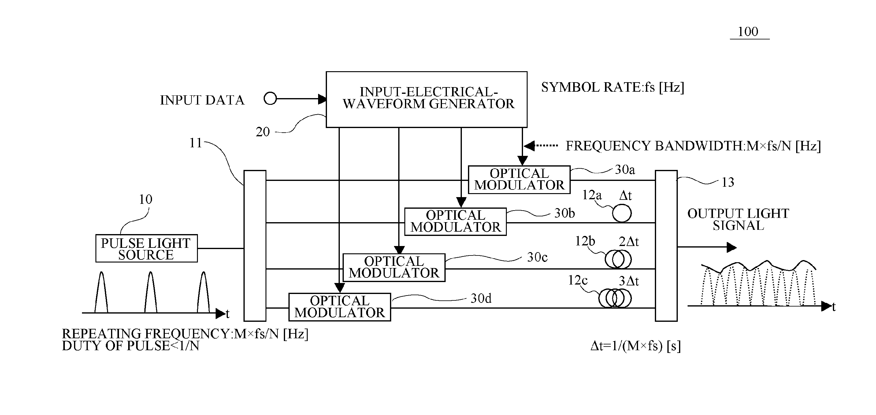
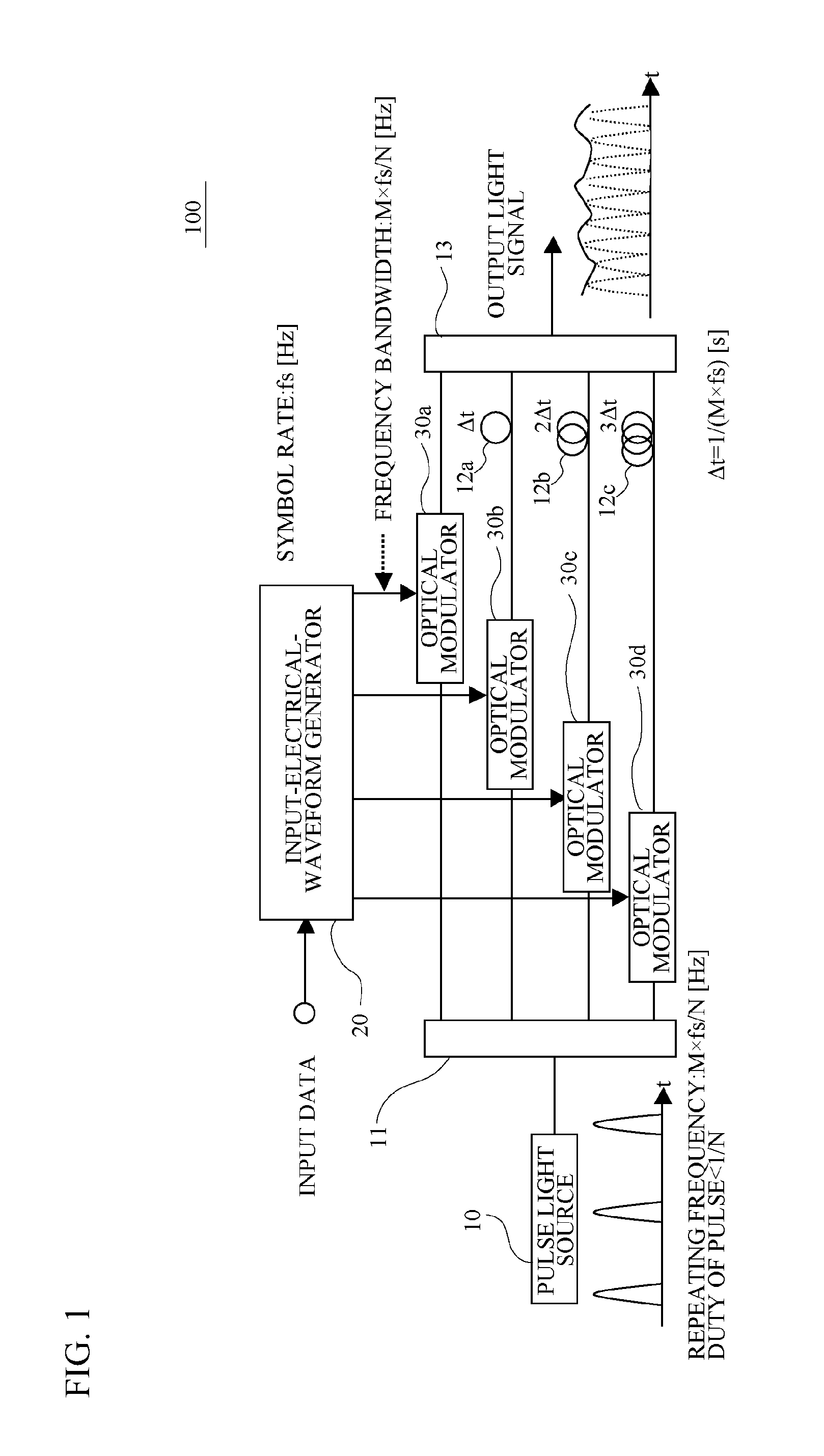
FIG. 1 illustrates a block diagram of an overall structure of an optical transmitter 100 in accordance with a first embodiment. As illustrated in FIG. 1, the optical transmitter 100 has a pulse light source 10, a divider 11, an input-electrical-waveform generator 20, optical modulators 30a to 30d, delays 12a to 12c and a composer 13.

The pulse light source 10 outputs a pulsed optical signal. For example, a semiconductor laser having a modulator integrally is used as the pulse light source 10. A repeating frequency of the pulsed optical signal from the pulse light source 10 is set to be M×fs / N [Hz]. A duty of the pulse of the pulse light source 10 is set to be less than 1 / N. The “fs” is a symbol rate [Hz] of an input data signal fed into the optical transmitter 100. The “M” is an integer that is equal to 1 or more. The “N” is a division number of an optical signal divided by the divider 11 and is an integer that is equal to 2 or more.

The divider 11 is an optical co...

second embodiment

FIG. 7 illustrates a block diagram of an overall structure of an optical transmitter and receiver 300 in accordance with a second embodiment. As illustrated in FIG. 7, the optical transmitter and receiver 300 has an optical receiver 200 and the optical transmitter 100 in accordance with the first embodiment. Further, the optical transmitter and receiver 300 has a repeating frequency controller 70. The optical transmitter and receiver 300 is located at each telephone office. An optical signal received by the optical receiver 200 is subjected to a given processing and is transmitted from the optical transmitter 100.

In the optical transmitter 100, a divider 18 is provided between the pulse light source 10 and the divider 11. The divider 18 divides an output light of the pulse light source 10. The divider 18 inputs one of the divided lights into the divider 11 and inputs the other into the repeating frequency controller 70. The repeating frequency controller 70 changes the repeating fre...


PUM


Abstract

An optical transmitter includes: a pre-compensator calculating an electrical field of an optical signal subjected to an electronic pre-compensation with respect to an input digital signal; a parallelizer parallelizing the electrical field of the optical signal calculated by the pre-compensator; a plurality of optical modulators modulating an optical signal based on each of parallelized electrical fields of optical signals; and a time-division multiplexer time-division-multiplexing an optical signal output from the plurality of the optical modulators.

Description

CROSS-REFERENCE TO RELATED APPLICATIONThis application is based upon and claims the benefit of priority of the prior Japanese Patent Application No. 2009-247816, filed on Oct. 28, 2009, the entire contents of which are incorporated herein by reference.FIELDA certain aspect of embodiments described herein relates to an optical transmitter, an optical transmitter and receiver system, an optical transmitting method and an optical transmitting and receiving method.BACKGROUNDIt is known that electronic pre-compensation is effective as a technology compensating for linear waveform distortion and non-linear waveform distortion of an optical transmission link. The technology is disclosed in U.S. Patent Application Publication No. 2004 / 0197103.However, the technology needs high-speed electronic devices for generating an optical signal at high symbol rate subjected to the electronic pre-compensation.SUMMARYAccording to an aspect of the present invention, there is provided an optical transmitt...

Claims


Application Information

Patent Timeline
IPC IPC(8): H04J14/08H04J14/06H04B10/2507H04B10/40H04B10/2513H04B10/2543H04B10/50H04B10/516H04B10/524H04B10/58H04B10/60
CPCH04B10/2569H04B10/5053H04B10/516H04J14/086H04J14/002H04J14/06H04B2210/254
Inventor ODA, SHOICHIROHOSHIDA, TAKESHITANIMURA, TAKAHITO
Owner FUJITSU LTD
Why Eureka
Try Eureka