Planar element, and touch switch

Inactive Publication Date: 2011-05-05
GUNZE LTD
View PDF19 Cites 315 Cited by
  • Summary
  • Abstract
  • Description
  • Claims
  • Application Information

AI Technical Summary

Benefits of technology

[0021]The present invention provides a touch switch having two ITO-free electrode layers bonded to each other,

Problems solved by technology

This results in an increase in the size of the touch switch, along with an increase in the resistance between terminals of

Method used


Image

  • Planar element, and touch switch
  • Planar element, and touch switch
  • Planar element, and touch switch

Examples


first embodiment

[0044]A touch switch according to a first embodiment of the present invention is described with reference to the drawings. The touch switch is a capacitive touch switch mounted to a front side of a display device. A black matrix forming a grid pattern of horizontal and vertical lines is formed in the display device.

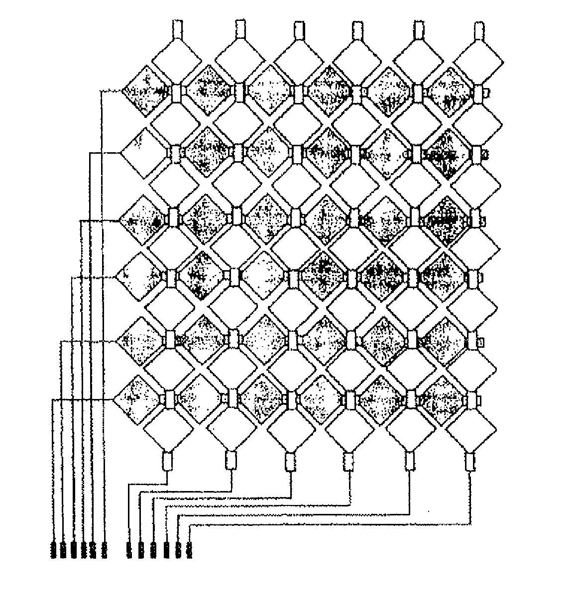
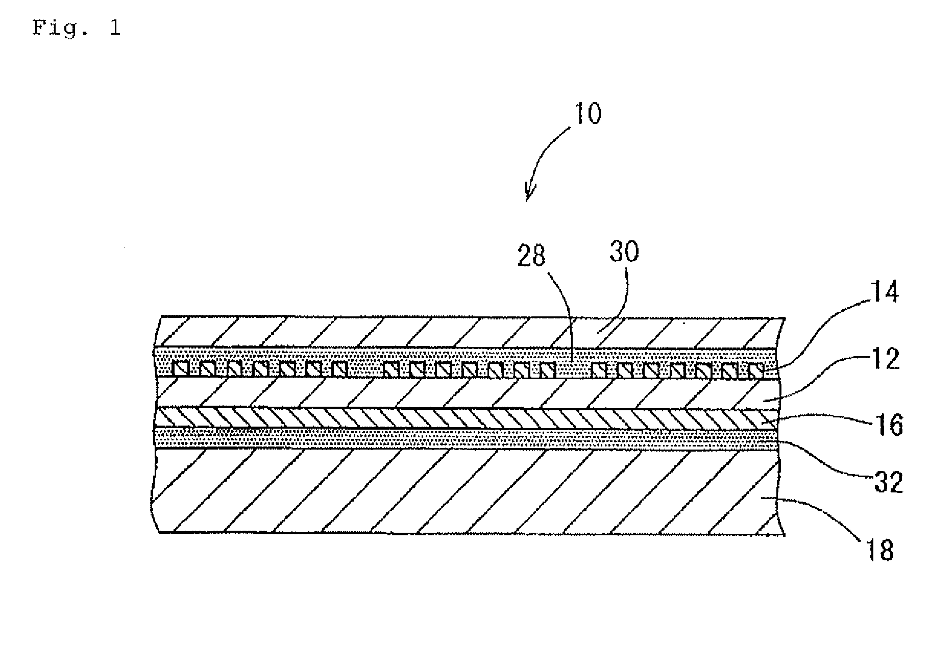
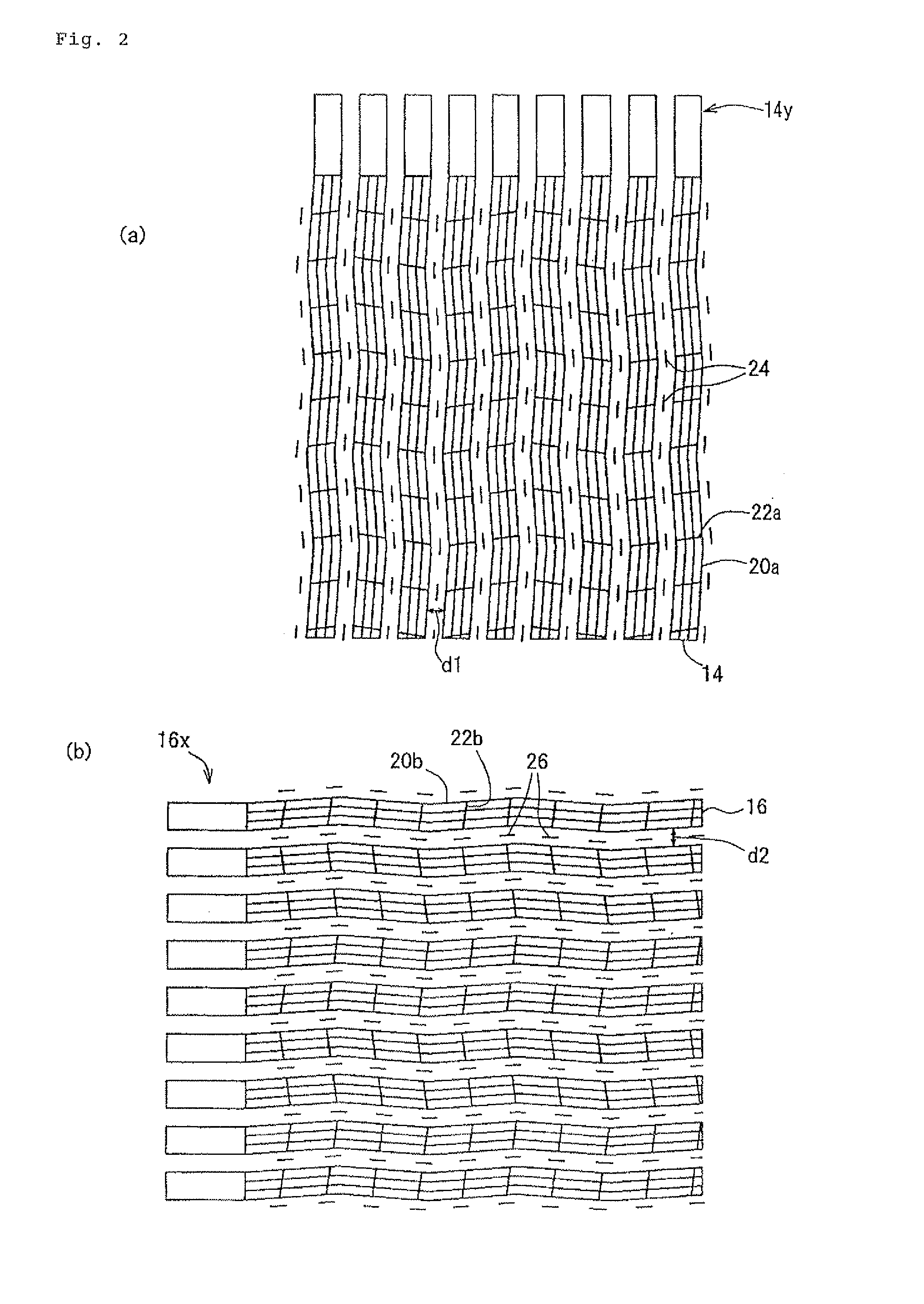
[0045]A touch switch 10 shown in FIG. 1 includes a substrate 12, first electrodes 14 formed on one side of the substrate 12, and second electrodes 16 formed on the other side of the substrate 12. In the description, the “one side” of the substrate 12 is an upper side, and the “other side” of the substrate 12 is a lower side, which is mounted to a display device 18.

[0046]The substrate 12 is a dielectric substrate. Examples of materials of the substrate 12 include transparent materials such as glass, polyester, polyethylene terephthalate, polycarbonate, polymethylmethacrylate, polyethylene naphthalate, etc. In the case of glass, the thickness is about 0.1 to 2 mm. In the ca...

second embodiment

[0078]Hereinbelow, a second embodiment of the present invention is described with reference to the attached drawings. Note that none of the drawings reflects the actual size. They are partially enlarged or reduced in order to facilitate the understanding of the structures.

[0079]FIG. 10 is an enlarged schematic cross-sectional diagram of the main components of a touch switch according to a second embodiment of the present invention. This touch switch 105 is a capacitive touch switch, and includes, as shown in FIGS. 11 and 12, a first planar body 101 in which a mesh-like electrode 112 is formed on one side of a substrate 111, and a second planar body 102 in which a mesh-like electrode 122 is formed on one side of a substrate 121. Note that FIG. 11 is a plan view of the first planar body 101, and FIG. 12 is a plan view of the second planar body 102. The first planar body 101 and the second planar body 102 are integrally bonded via an adhesive layer 103 in such a manner that the mesh-li...


PUM


Abstract

The present invention provides a touch switch having two ITO-free electrode layers that are bonded together, the touch switch having good visibility, and a planar body that forms such a touch switch. The planar body includes a mesh-like electrode formed in a mesh shape by multiple conductor lines L on one side of a substrate, in which the mesh-like electrode is separated into multiple conductive areas disposed at intervals, and non-conductive areas each disposed between each of the conductive areas; each non-conductive area has multiple cutting portions that cut the conductor lines L, and each non-conductive area insulates between the adjacent conductive areas by the cutting portions.

Description

TECHNICAL FIELD[0001]The present invention relates to a planar body and a touch switch.BACKGROUND ART[0002]These days, in the field of computers and electronic devices, operations performed using the contents displayed on a display device, rather than using buttons, have been increasingly developed. To perform such operations, a touch switch is arranged at the front side of the display device, and a touch position is detected. The types of touch switches include a resistive type, a surface acoustic wave type, an infrared type, and the like. There is also a capacitive type, in which a position is detected by a variation in capacitance caused by a touch of a finger and / or proximity of a finger. For example, Patent Literature 1 discloses a capacitive touch switch having a matrix electrode (a two-layer structure in X-direction and Y-direction), as shown in FIGS. 19 and 20.[0003]A detailed description is provided with reference to FIG. 21, which is a schematic plan diagram schematically ...

Claims


Application Information

Patent Timeline
IPC IPC(8): G06F3/044H03K17/975
CPCG06F3/044H03K17/9622G06F2203/04112G06F3/0445G06F3/0446G06F2203/04103
Inventor KONO, KATSUMASAMIZUMOTO, HIDEAKI
Owner GUNZE LTD
Why Eureka
Try Eureka