Light emitting diode having electrode extensions for current spreading

Active Publication Date: 2011-05-19
SEOUL VIOSYS CO LTD
View PDF16 Cites 17 Cited by
  • Summary
  • Abstract
  • Description
  • Claims
  • Application Information

AI Technical Summary

Benefits of technology

[0017]Exemplary embodiments of the present invention provide a light emitting diode cap

Problems solved by technology

However, since the transparent electrode layer absorbs light, the thickness thereof is limited.
As a result, the transparent electrode layer has a limited current spreading ability.
Howeve

Method used


Image

  • Light emitting diode having electrode extensions for current spreading
  • Light emitting diode having electrode extensions for current spreading
  • Light emitting diode having electrode extensions for current spreading

Examples


experimental example

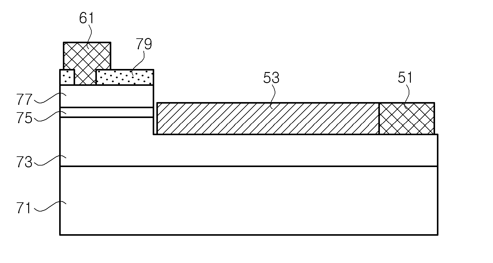
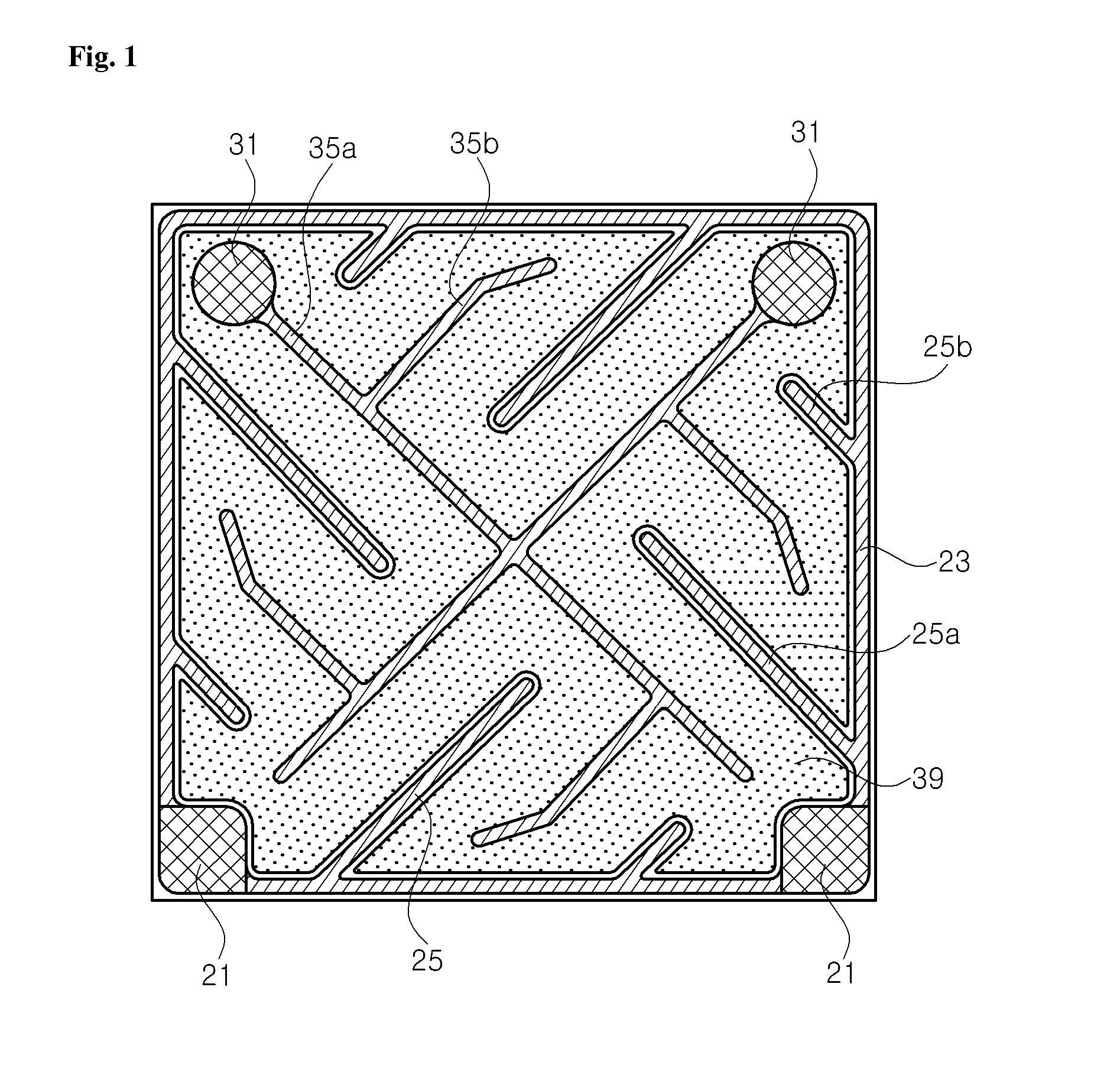
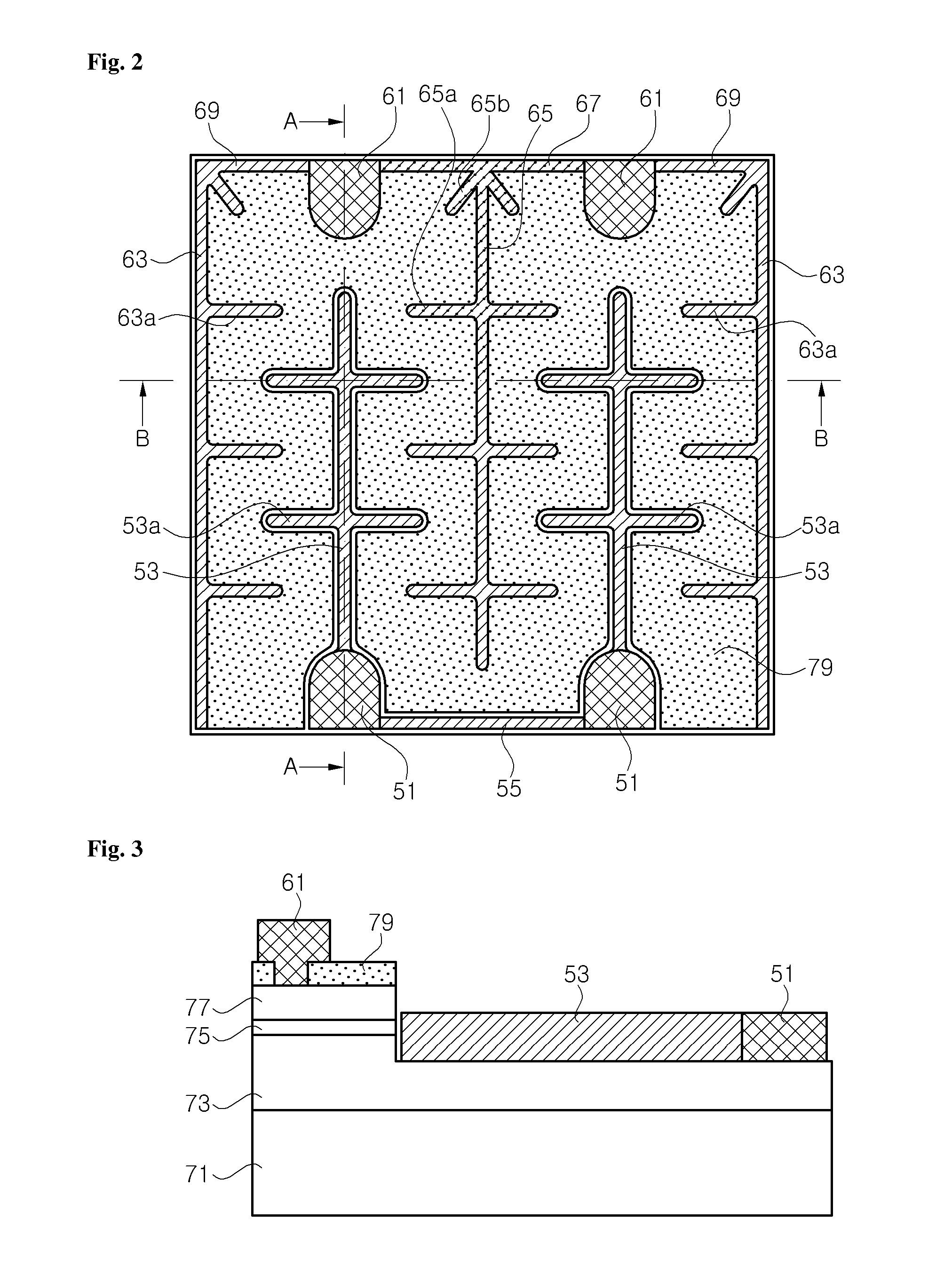
[0059]The stacked structure of the light emitting diode and the transparent electrode layer were formed under the same conditions, and the light emitting diodes shown in FIG. 1 (Comparative Example), FIG. 2 (Example 1), and FIG. 5 (Example 2) were manufactured, and then the light emitting area, the light output, and the forward voltage at 350 mA were measured, which are listed in the following Table 1. The size of the light emitting diode used in the experimental example was 1.1 mm×1.1 mm and the area of the active layer and the area of the second electrode pads and the second extensions were obtained by being calculated from a layout, the light emitting area was obtained by subtracting the area of the second electrode pads and the second extensions from the area of the active layer, and the relative value was shown based on the light emitting diode of FIG. 1.

TABLE 1ComparativeExampleExample 1Example 2Area of active layer100105.07104.78Sum of areas of second100138.66117.68electrode ...


PUM


Abstract

An exemplary embodiment of the present invention discloses a light emitting diode including a substrate having a first edge and a second edge opposite to each other, a light emitting structure disposed on the substrate, the light emitting structure including a first semiconductor layer and a second semiconductor layer, a plurality of first electrode pads arranged on an upper surface of the first semiconductor layer, the first electrode pads arranged in a vicinity of the first edge, a plurality of second electrode pads arranged on the second semiconductor layer, the second electrode pads arranged in a vicinity of the second edge, a plurality of first extensions, each first extension extending from a first electrode pad, and a plurality of second extensions, each second extension extending from a second electrode pad. The first extensions include intrusion parts extending in a direction from the first edge to the second edge, wherein the intrusion parts are spaced apart from each other and not connecting with the second electrode pads. Further, the second extensions include intrusion parts extending in a direction from the second edge to the first edge, wherein the first extension intrusion parts each extend into a region between two of the second extension intrusion parts.

Description

CROSS-REFERENCE TO RELATED APPLICATION[0001]This application claims priority from and the benefit of Korean Patent Application No. 10-2009-0110097, filed on Nov. 16, 2009, which is hereby incorporated by reference for all purposes as if fully set forth herein.BACKGROUND OF THE INVENTION[0002]1. Field of the Invention[0003]The present invention relates to a light emitting diode, and more particularly, to a light emitting diode having electrode extensions for current spreading.[0004]2. Discussion of the Background[0005]Gallium nitride (GaN)-based light emitting diodes (LEDs) have been used for is various applications, such as a natural color LED display, an LED traffic signal, a white LED, or the like. Also, a high-efficiency white LED is expected to replace a fluorescent lamp. In particular, the efficiency of the white LED reaches a similar level to the efficiency of the general fluorescent lamp.[0006]The GaN-based light emitting diode is generally formed by growing epitaxial layers ...

Claims


Application Information

Patent Timeline
IPC IPC(8): H01L33/62
CPCH01L33/38H01L33/20
Inventor KIM, KYOUNG WANMOON, SOO YOUNGLEE, KYU HOYOON, YEO JINYANG, JEONG HEESEO, WON CHEOL
Owner SEOUL VIOSYS CO LTD
Why Eureka
Try Eureka