Semiconductor device

a technology of semiconductor devices and semiconductors, applied in the direction of semiconductor devices, basic electric elements, electrical equipment, etc., can solve the problems of adversely affecting the operational current characteristic of ldmos transistors, breakdown voltage characteristics may be adversely impacted,

Active Publication Date: 2011-05-19
KEY FOUNDRY CO LTD
View PDF3 Cites 15 Cited by
  • Summary
  • Abstract
  • Description
  • Claims
  • Application Information

AI Technical Summary

Benefits of technology

[0028]The semiconductor device may further comprise a buried impurity layer of second conductivity type formed between the substrate and the semiconductor layer, the buried impurity layer having an impurity concentration that is higher than the uniform impurity concentration of the first region of the semiconductor layer.
[0029]The buried impurity layer may include a first impurity layer region and a second impurity layer region. The first impurity layer region may have an impurity concentration that is substantially uniform throughout the first impurity layer region and that is higher than the uniform impurity concentration of the first region of the semiconductor layer. The second impurity layer region may have impurity concentration that varies across the second impurity layer region in such a manner that the impurity concentration of the second impurity layer region is the highest at a region boundary between the first and second impurity layer regions, and is the lowest farthest away from the region boundary.

Problems solved by technology

When the impurity doping concentration is decreased in the N-type deep well 12 or in the drift region D in order to secure a sufficiently high breakdown voltage, the specific on resistance increases to thereby adversely affecting the operational current characteristic of the LDMOS transistor.
Conversely, when the impurity doping concentration is increased in the N-type deep well 12 or in the drift region D in order to secure suitable operational current characteristic, the breakdown voltage characteristic may be adversely impacted.

Method used


Image

  • Semiconductor device
  • Semiconductor device
  • Semiconductor device

Examples


Embodiment Construction

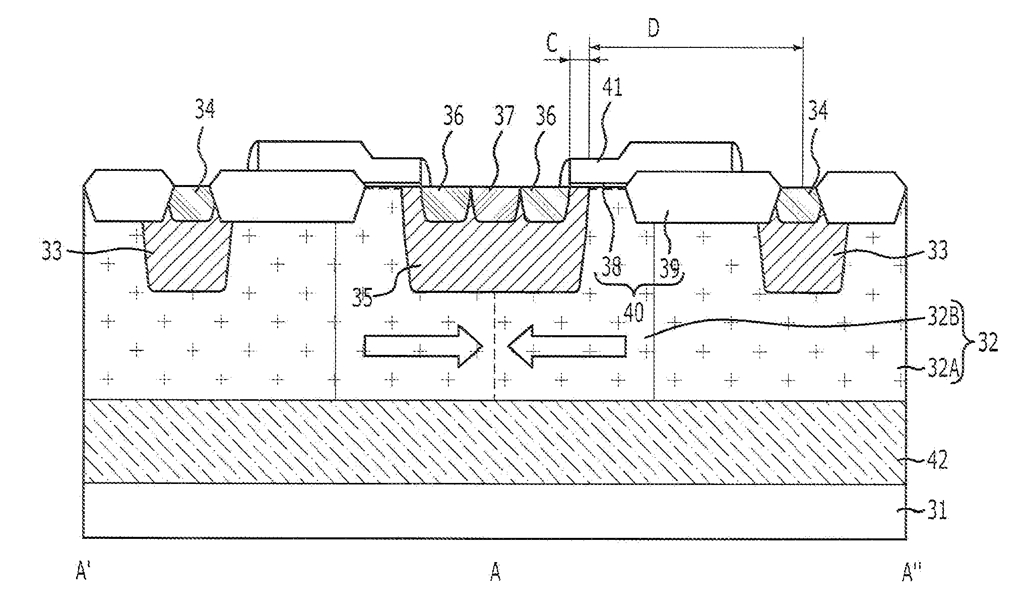
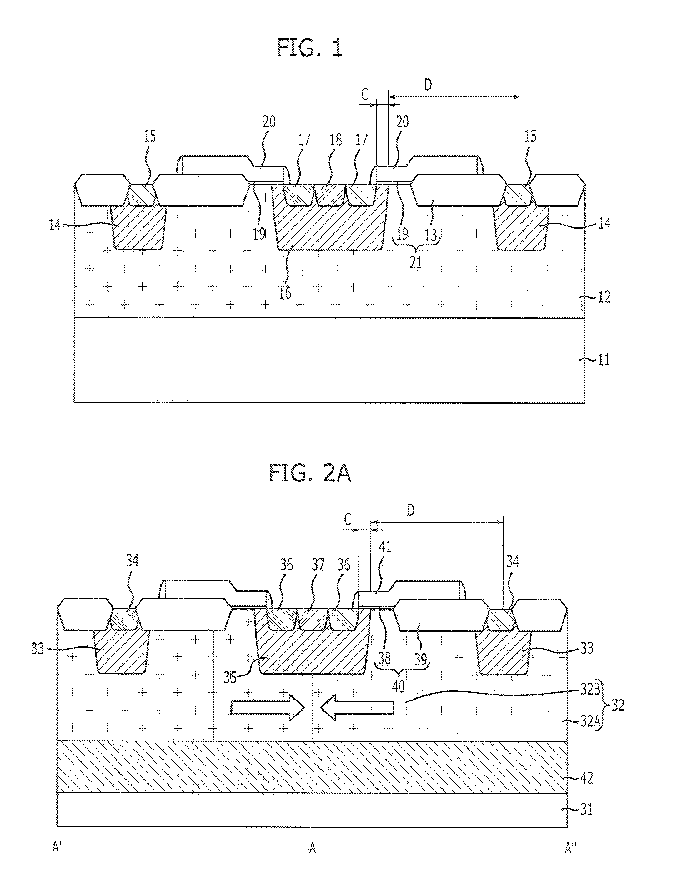
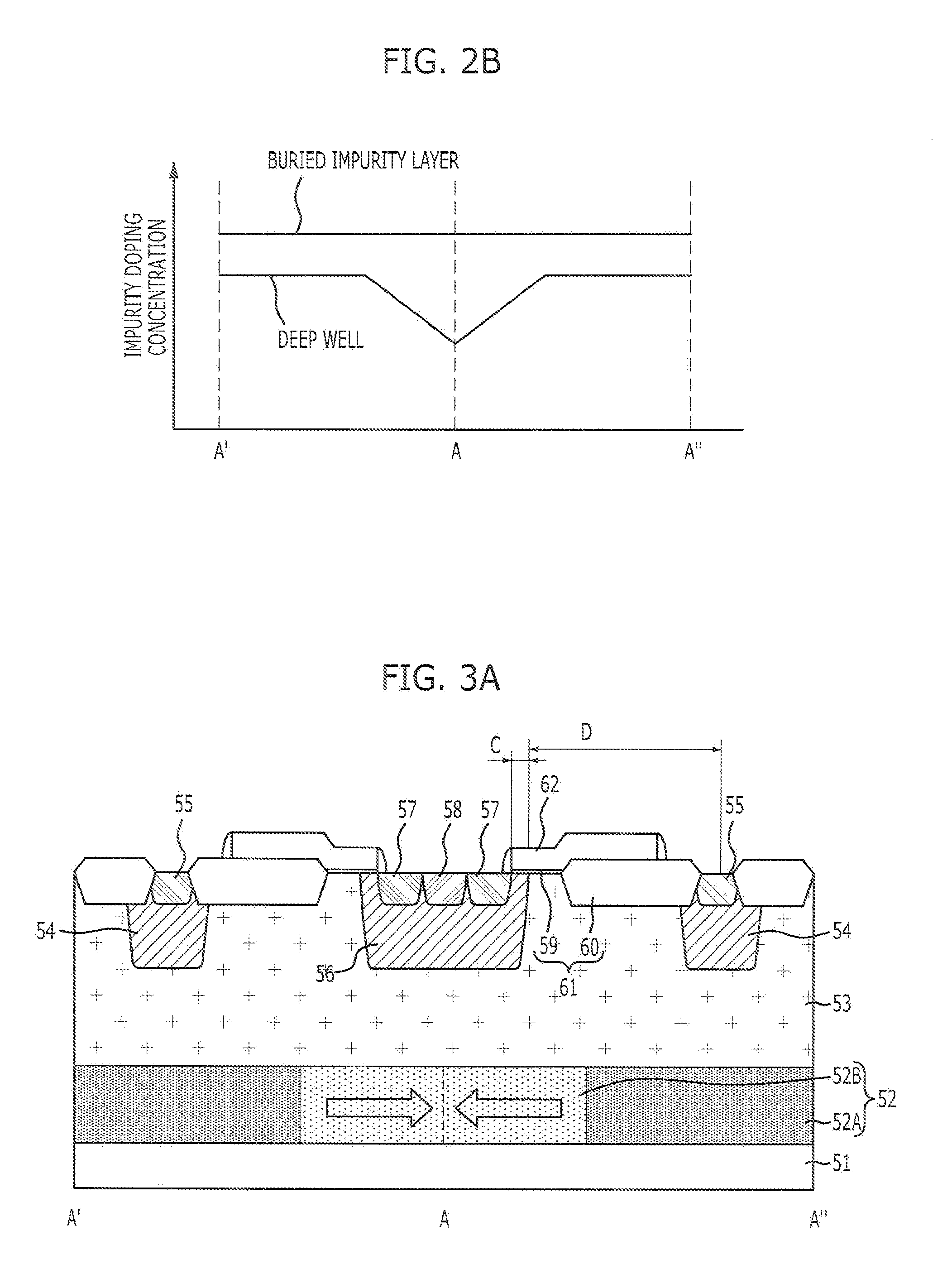
[0038]Several embodiments of the present disclosure will be described below in detail with reference to the accompanying drawings. It should be understood that these embodiments are not intended, and should not be construed, to limit the full scope of the present disclosure, and that aspects and features of the present disclosure may be carried out with different configurations and elements than specifically detailed in those embodiments described herein. Rather, these embodiments are provided so that this disclosure will be thorough and complete, and will fully convey the scope of the present disclosure to those skilled in the art. Throughout the disclosure, like reference numerals refer to like parts throughout the various figures and embodiments of the present invention. The drawings are not necessarily to scale and in some instances, proportions may have been exaggerated for the sake of clarity. When a first layer is referred to as being “on” a second layer or “on” a substrate, ...


PUM


Abstract

A semiconductor device includes a second conductive-type deep well configured above a substrate. The deep well includes an ion implantation region and a diffusion region. A first conductive-type first well is formed in the diffusion region. A gate electrode extends over portions of the ion implantation region and of the diffusion region, and partially overlaps the first well. The ion implantation region has a uniform impurity concentration whereas the impurity concentration of the diffusion region varies from being the highest concentration at the boundary interface between the ion implantation region and the diffusion region to being the lowest at the portion of the diffusion region that is the farthest away from the boundary interface.

Description

CROSS-REFERENCE TO RELATED APPLICATIONS[0001]The present application claims priority 35 U.S.C. §119 of Korean Patent Application No. 10-2009-110926, filed on Nov. 17, 2009, which is incorporated herein by reference in its entirety.TECHNICAL FIELD[0002]The present disclosure relates generally to fabrication of a semiconductor device, and, more particularly, to the fabrication of a high-voltage MOS transistor.BACKGROUND OF RELATED ART[0003]A lateral double-diffused MOS (LDMOS) transistor based on planar diffusion technology is generally used as a high-voltage MOS transistor. Owing to the higher input impedance in comparison to a bipolar transistor, an LDMOS transistor can realize a high power gain and / or a simpler gate driving circuit. Since an LDMOS transistor is a unipolar device, it advantageously exhibits little or no time delay when being turned off. The time delay usually originates from accumulated hydrophobic carriers.[0004]FIG. 1 is a cross-sectional view illustrative of a co...

Claims


Application Information

Patent Timeline
Patent Type & Authority Applications(United States)
IPC IPC(8): H01L29/78
CPCH01L29/0878H01L29/7816H01L29/66681H01L29/42368H01L21/18H01L21/265
Inventor CHA, JAE-HANLEE, KYUNG-HOKIM, SUN-GOOCHOI, HYUNG-SUKKIM, JU-HOCHAE, JIN-YOUNGOH, IN-TAEK
Owner KEY FOUNDRY CO LTD
Why Eureka
Try Eureka