Electrophoresis display panel

a display panel and electrophoresis technology, applied in the field of electrophoresis display panels, can solve the problems of poor display quality of electrophoresis displays, and achieve the effect of effectively decreasing the photo curren

Active Publication Date: 2011-05-19
AU OPTRONICS CORP
View PDF5 Cites 5 Cited by
  • Summary
  • Abstract
  • Description
  • Claims
  • Application Information

AI Technical Summary

Benefits of technology

[0007]The present invention provides an electrophoresis display panel having a shielding pattern capable of ef

Problems solved by technology

After passing through the dielectric layer of the electrophoresis display film, the external light source beams on thin film transistors on the thin film transistor array substr

Method used


Image

  • Electrophoresis display panel
  • Electrophoresis display panel
  • Electrophoresis display panel

Examples


first embodiment

The First Embodiment

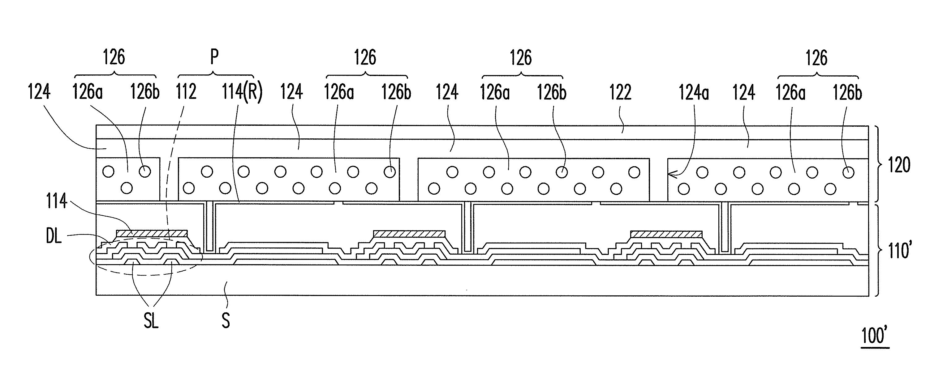
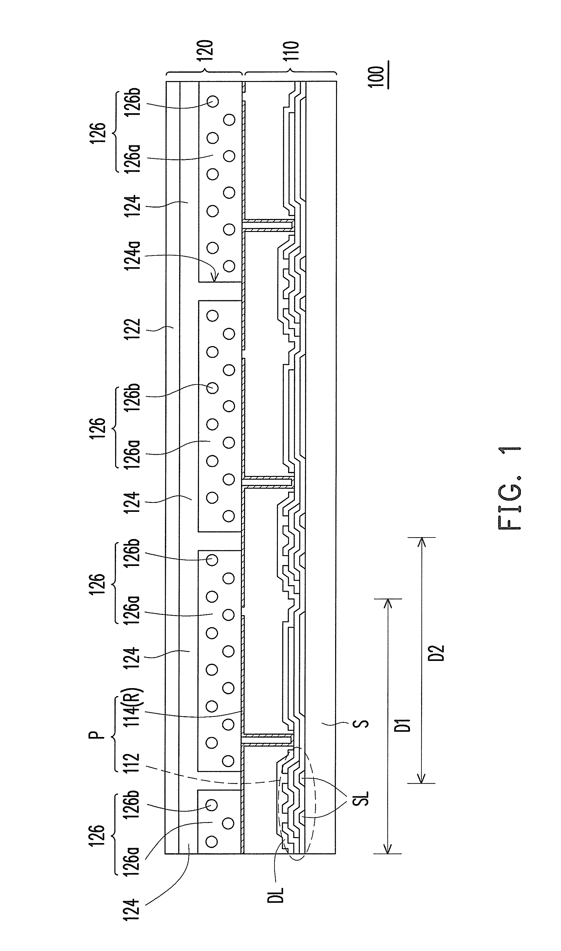
[0025]FIG. 1 schematic cross-sectional view showing an electrophoresis display panel according to the first embodiment of the present invention. Referring to FIG. 1, an electrophoresis display panel 100 of the present embodiment comprises an active device array substrate 110 and an electrophoresis display film 120. The active device array substrate 110 has a plurality of active devices 112 and a shielding pattern 114 covering the active devices 112. The electrophoresis display film 120 is disposed on the active device array substrate 110 and the electrophoresis display film 120 comprises a conductive layer 122, a dielectric layer 124 and a plurality of electrophoresis display mediums 126. As shown in FIG. 1, the dielectric layer 124 is disposed on the upper surface of the conductive layer 122 and has a plurality of micro-cups 124a arranged in an array on the bottom surface of the dielectric layer 124. Also, the dielectric layer 124 is disposed between the conduct...

second embodiment

The Second Embodiment

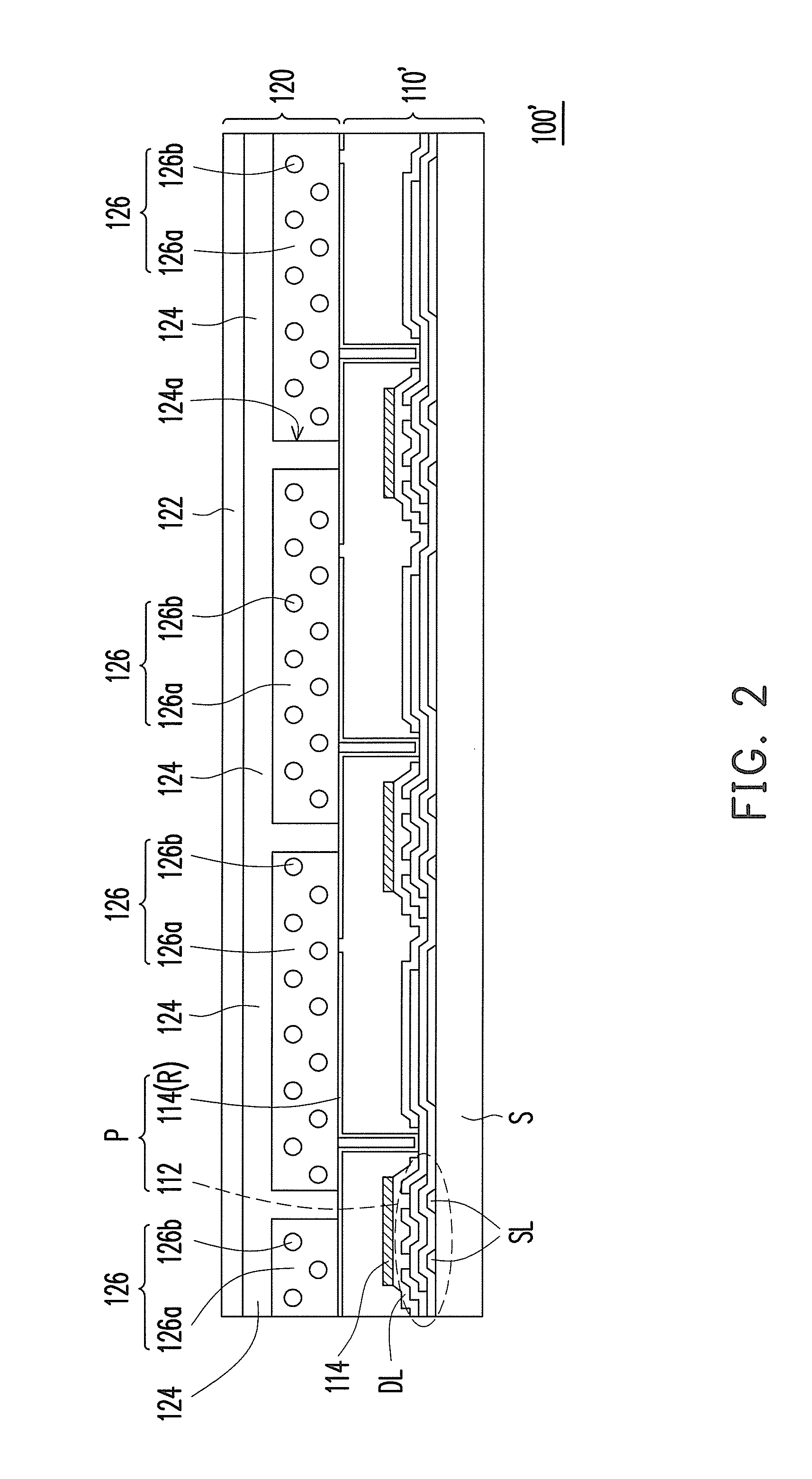
[0030]FIG. 2 schematic cross-sectional view showing an electrophoresis display panel according to the second embodiment of the present invention. As shown in FIG. 2, an electrophoresis display panel 100′ of the present embodiment is similar to the electrophoresis display panel 100 described in the first embodiment. However, the difference between the electrophoresis display panel 100′ and electrophoresis display panel 100 is that the shielding pattern 114 in the active device array substrate 110′ of the present invention is located between the pixel electrodes PE and the active devices 112, and the active devices 112 and the pixel electrodes PE together form a plurality of pixels P. In other words, the shielding pattern 114 and the pixel electrodes PE are not parts of the same film layer, which is different from the reflective pixel electrodes R of the first embodiment.

[0031]Accordingly, the aforementioned shielding pattern 114 of the present embodiment can be a...


PUM


Abstract

An electrophoresis display panel including an active device array substrate and an electrophoresis display film is provided. The active device array substrate includes a plurality of active devices and a shielding pattern. The electrophoresis display film is disposed on the active device array substrate. The electrophoresis display film includes a conductive layer, a dielectric layer and a plurality of electrophoresis display mediums. The dielectric layer is disposed on the conductive layer and has a plurality of micro-cups arranged in area array. The dielectric layer is between the conductive layer and the active device array substrate. Light passing through the dielectric layer is prevented from irradiating onto the active devices by the shielding pattern. In addition, the electrophoresis display mediums are filled within the micro-cups, respectively.

Description

CROSS-REFERENCE TO RELATED APPLICATION[0001]This application claims the priority benefit of Taiwan application serial no. 98138842, filed on Nov. 16, 2009. The entirety of the above-mentioned patent application is hereby incorporated by reference herein and made a part of specification.BACKGROUND OF THE INVENTION[0002]1. Field of the Invention[0003]The present invention is related to an electrophoresis display panel, and more particular to an electrophoresis display panel with a shielding pattern.[0004]2. Description of Related Art[0005]Currently, due to the continuous advancement and research of the display technologies, the products such as electrophoresis displays, liquid crystal displays, plasma displays and organic-light-emitting diode displays are commercialized and applied to the display devices with various dimensions and standards. With the increasing of the use of the portable electronic devices, the flexible displays, such as electronic papers and electronic books, have g...

Claims


Application Information

Patent Timeline
IPC IPC(8): G02F1/167G02F1/1677
CPCG02F1/1362G02F2001/1672G02F1/167G02F1/1681G02F1/1677
Inventor WEI, CHUAN-SHENGHUANG, SHENG-WENCHEN, PEI-MINGCHEN, CHUN-HSIUNHUANG, WEI-MING
Owner AU OPTRONICS CORP
Why Eureka
Try Eureka