Method for manufacturing a suspended membrane and dual-gate mos transistor

Active Publication Date: 2011-05-26
STMICROELECTRONICS (CROLLES 2) SAS
View PDF3 Cites 7 Cited by
  • Summary
  • Abstract
  • Description
  • Claims
  • Application Information

AI Technical Summary

Benefits of technology

[0012]An object of an embodiment of the present invention is to provide a method for manufacturing

Problems solved by technology

A hydrogen chloride gas at high temperature used for this s

Method used


Image

  • Method for manufacturing a suspended membrane and dual-gate mos transistor
  • Method for manufacturing a suspended membrane and dual-gate mos transistor
  • Method for manufacturing a suspended membrane and dual-gate mos transistor

Examples


Embodiment Construction

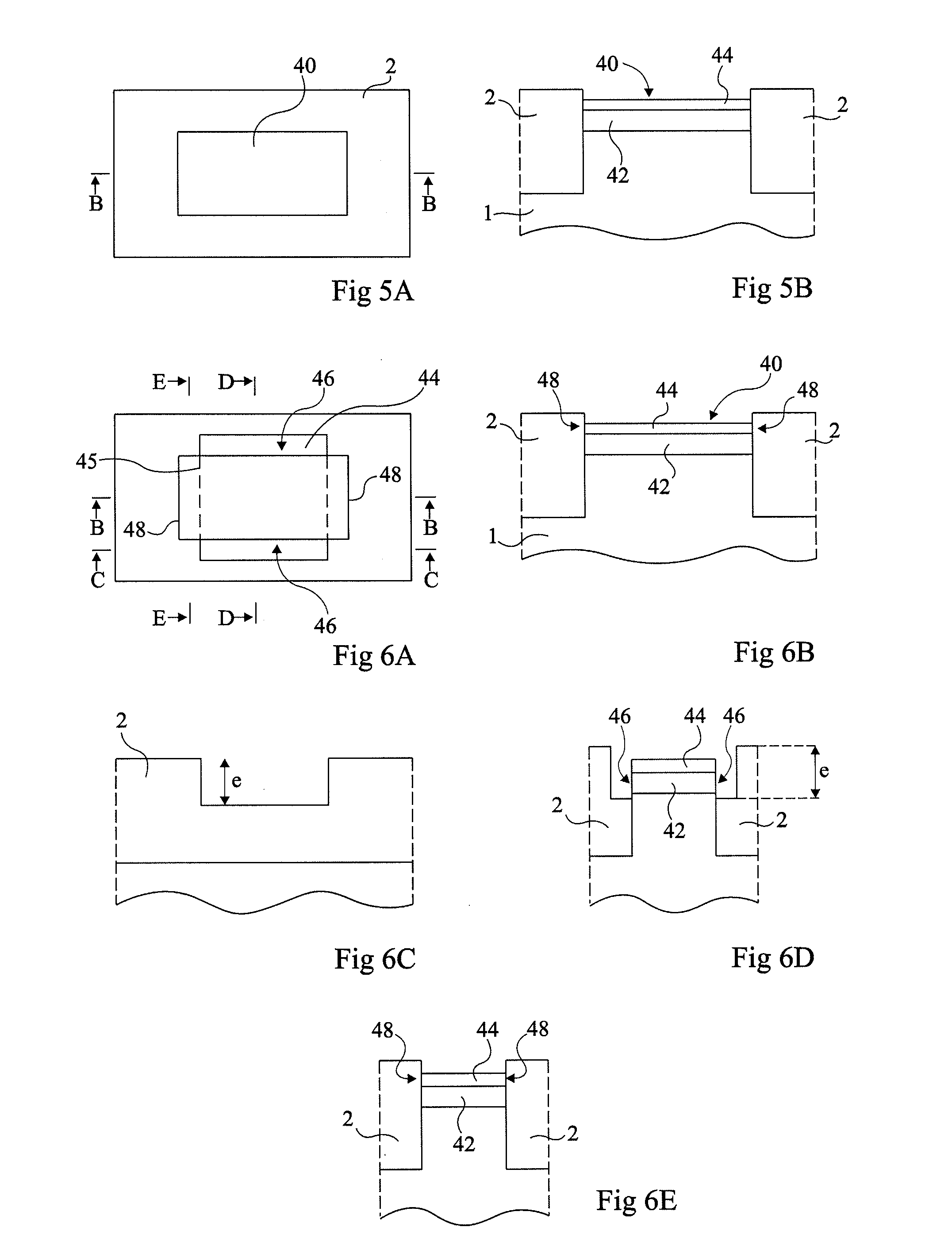
[0045]For clarity, the same elements have been designated with the same reference numerals in the different drawings and, further, as usual in the representation of integrated circuits, the various drawings are not to scale.

[0046]FIGS. 5A and 5B show a solid substrate 1 made of a single-crystal semiconductor material, for example, silicon, in which an insulating ring 2 delimiting an active area 40 have formed. Insulating ring 2, for example, is silicon oxide. Material is removed from area 40 by partial etching of the silicon, for example, by a hydrogen chloride gas at high temperature down to a depth lower than that of the insulating ring. A sacrificial layer 42, for example, made of silicon-germanium, followed by a single-crystal semiconductor layer 44, for example, made of silicon, have been epitaxially formed. The upper surface of layer 44 is at the level of the upper surface of insulating ring 2 or slightly below. The thickness of sacrificial layer 42 for example ranges between ...


PUM


Abstract

A method for manufacturing a suspended membrane in a single-crystal semiconductor substrate, including the steps of: forming in the substrate an insulating ring delimiting an active area, removing material from the active area, successively forming in the active area a first and a second layers, the second layer being a single-crystal semiconductor layer, etching a portion of the internal periphery of said ring down to a depth greater than the thickness of the second layer, removing the first layer so that the second layer formed a suspended membrane anchored in the insulating ring.

Description

CROSS REFERENCE TO RELATED APPLICATIONS[0001]This application claims the priority benefit of French patent application Ser. No. 09 / 58280, filed on Nov. 23, 2009, entitled “Method for Manufacturing a Suspended Membrane and Dual-Gate MOS Transistor,” which is hereby incorporated by reference to the maximum extent allowable by law.BACKGROUND OF THE INVENTION[0002]1. Field of the Invention[0003]The present invention relates to integrated circuits. It more specifically relates to methods for manufacturing electronic components designated as SON in the art (for Silicon On Nothing).[0004]2. Discussion of the Related Art[0005]MOS transistors are currently formed on an SOI-type substrate (for Silicon On Insulator). Since the cost of this substrate is not negligible, it has been provided to locally form, in a solid substrate, a buried silicon oxide layer under a single-crystal silicon film on which the transistor will be formed.[0006]FIGS. 1A to 4B illustrate successive steps of the forming o...

Claims


Application Information

Patent Timeline
IPC IPC(8): H01L29/786H01L21/762
CPCH01L29/786H01L29/78648
Inventor MONFRAY, STEPHANESKOTNICKI, THOMAS
Owner STMICROELECTRONICS (CROLLES 2) SAS
Why Eureka
Try Eureka