Solid-state imaging device, method for manufacturing solid-state imaging device, method for manufacturing solid-state imaging element, and semiconductor device

a solid-state imaging and manufacturing method technology, applied in semiconductor devices, semiconductor/solid-state device details, electrical devices, etc., can solve problems such as disadvantageous degradation of yield, and achieve the effect of reducing chip propagation and improving manufacturing yield

Active Publication Date: 2011-06-02
SONY CORP
View PDF4 Cites 35 Cited by
  • Summary
  • Abstract
  • Description
  • Claims
  • Application Information

AI Technical Summary

Benefits of technology

[0020]The groove which is provided between the blade region in the scribe line region and the semiconductor chip, in the first semiconductor substrate and penetrates through the first semiconductor substrate can suppress chipping propagating at an interface between the first semiconductor substrate and the wiring layer.
[0021]In the solid-state imaging device, the method for manufacturing a solid-state imaging device, the method for manufacturing a solid-state imaging element, and the semiconductor device according to the embodiments of the present invention, chipping can be suppressed and therefore improvement of a manufacturing yield can be realized.

Problems solved by technology

When the chipping reaches a semiconductor chip region, a product defect occurs and a yield may be disadvantageously degraded.

Method used


Image

  • Solid-state imaging device, method for manufacturing solid-state imaging device, method for manufacturing solid-state imaging element, and semiconductor device
  • Solid-state imaging device, method for manufacturing solid-state imaging device, method for manufacturing solid-state imaging element, and semiconductor device
  • Solid-state imaging device, method for manufacturing solid-state imaging device, method for manufacturing solid-state imaging element, and semiconductor device

Examples


embodiment

1. Embodiment

2. Another Embodiment

3. Modification

1. Embodiment

Configuration of Solid-State Imaging Device

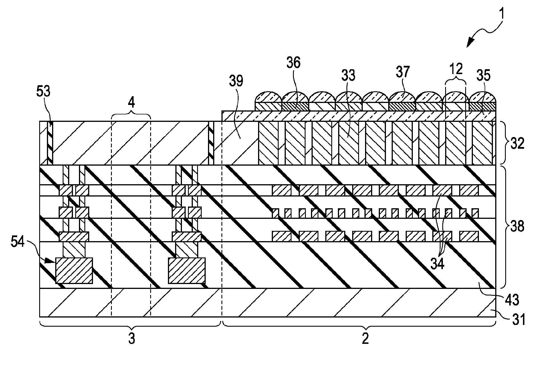
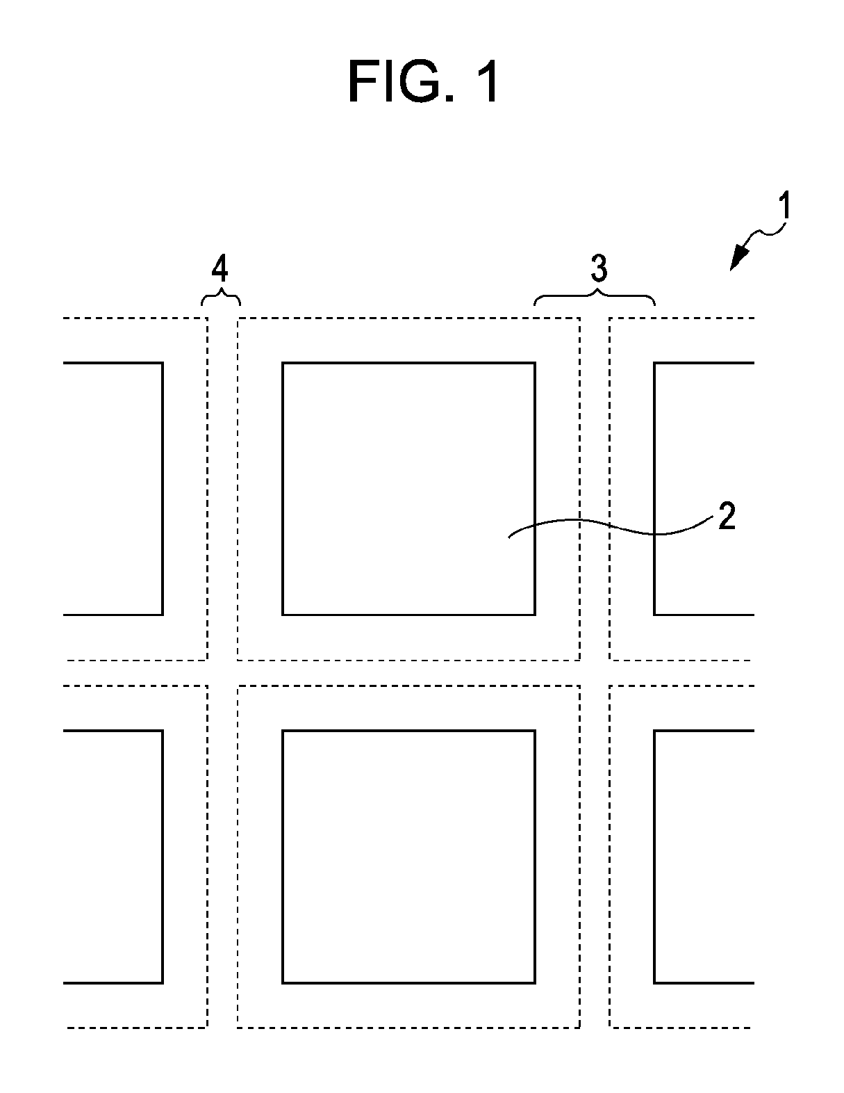
[0043]FIG. 1 schematically illustrates an example of a solid-state imaging device to which an embodiment of the present invention is applied. In a solid-state imaging device 1 shown in FIG. 1, a plurality of back-illuminated type solid-state imaging elements (semiconductor chips) 2 are formed and a scribe line 3 is provided in a gap between the solid-state imaging elements 2. Further, a blade region 4 is provided in the scribe line 3.

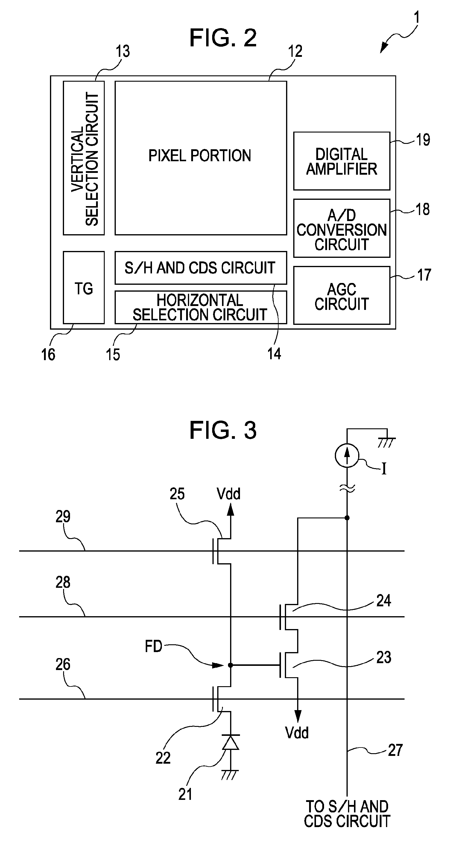
[0044]The solid-state imaging device 1 includes a pixel portion 12 and a peripheral circuit portion that are mounted on a single semiconductor substrate, as shown in FIG. 2. The peripheral circuit portion includes a vertical selection circuit 13, a sample-hold and correlated double sampling (S / H and CDS) circuit 14, a horizontal selection circuit 15, a timing generator (TG) 16, an automatic gain control (AGC) circuit 17, an A / D conversion circuit 18,...


PUM


Abstract

A solid-state imaging device includes a semiconductor substrate configured to include a solid-state imaging element that is provided with a photoelectric conversion region, and a scribe line region that is provided along a periphery of the solid-state imaging element, a wiring layer that is formed to be layered on the semiconductor substrate, a support substrate that is formed to be layered on the wiring layer, and a groove that is provided between a blade region in the scribe line region and the solid-state imaging element, in the semiconductor substrate and penetrates through the semiconductor substrate.

Description

BACKGROUND OF THE INVENTION[0001]1. Field of the Invention[0002]The present invention relates to a solid-state imaging device, a method for manufacturing a solid-state imaging device, a method for manufacturing a solid-state imaging element, and a semiconductor device. In particular, the present invention relates to a solid-state imaging device in which a plurality of semiconductor substrates are layered, a method for manufacturing the solid-state imaging device, a method for manufacturing a solid-state imaging element in which a plurality of semiconductor substrates are layered, and a semiconductor device.[0003]2. Description of the Related Art[0004]Commonly, in manufacturing of a semiconductor chip, after a plurality of semiconductor chips are formed on a wafer, the wafer is diced with a blade along a scribe line provided around the semiconductor chips so as to divide the wafer into individual semiconductor chips.[0005]For suppressing chipping occurring in the dicing with a blade,...

Claims


Application Information

Patent Timeline
Patent Type & Authority Applications(United States)
IPC IPC(8): H01L31/00H01L31/18H01L23/544
CPCH01L27/14603H01L27/14621H01L27/14627H01L27/14645H01L27/14683H01L2924/0002H01L27/14601H01L2924/00H01L27/14632H01L27/14636
Inventor KAWASHIMA, HIROYUKI
Owner SONY CORP
Why Eureka
Try Eureka