
Non-contact electronic device

a non-contact electronic and IC card technology, applied in the direction of electrical equipment, instruments, computing, etc., can solve the problems of erroneous data reception, data signal waveform disturbance, and the ability to suppress the reciprocal interference itself between the coils provided in the individual ic card, so as to achieve stable data communication without significant degradation of communication distance, suppress the variation of resonance frequency, and exclude the influence of the second coil

Inactive Publication Date: 2011-06-09
RENESAS ELECTRONICS CORP
View PDF2 Cites 8 Cited by
  • Summary
  • Abstract
  • Description
  • Claims
  • Application Information

AI Technical Summary

Benefits of technology

[0020]Mutual interference between the coils provided in IC cards can be reduced by applying the technology disclosed in Patent Document 2. This makes it possible to bring the resonance frequency of the resonance circuit formed by each antenna coil close to the carrier frequency. However, since it is necessary to fold back a base material with a coil formed therein and encircle one side of a magnetic core formed of a soft magnetic member or the like with it, it is difficult to reduce the thickness of the IC card.
[0021]It is an object of the invention to provide a non-contact electronic device that makes it possible to suppress variation in resonance frequency due to mutual interference between the coils provided in individual IC cards and facilitates reduction of the thickness of a housing.
[0022]It is another object of the invention to provide a non-contact electronic device that makes it possible to prevent significant degradation in communication distance when multiple IC cards are simultaneously used and facilitates reduction of the thickness of a housing.
[0025]The non-contact electronic device of the invention includes: a substrate; a first coil for antenna arranged in the substrate; a semiconductor integrated circuit device that is arranged in the substrate and carries out non-contact interface with an external source utilizing the first coil; and a second coil that comprises a resonance circuit together with the first coil and is shielded from external electromagnetic waves. For example, when there are multiple non-contact electronic devices mentioned above in a range within which a reader-writer device can communicate, the second coils provided in the individual non-contact electronic devices are not mutually influenced by each other. Therefore, even though the inductance or the like of each non-contact electronic device is equivalently increased, the influence of the second coil can be excluded. This makes it possible to ease a situation in which the resonance frequency of the resonance circuit formed by the coils of each non-contact electronic device is varied to a significantly low frequency as compared with cases where a non-contact electronic device is singularly used. With respect to the second coil, it only has to be shielded from external electromagnetic waves and it is unnecessary to provide a means for folding back a base material with a resonance coil formed therein and encircling one side of a magnetic core formed of a soft magnetic member or the like with it.
[0027]Even when multiple non-contact electronic devices are simultaneously used, it is possible to suppress variation in resonance frequency due to mutual interference between coils provided in individual non-contact electronic devices. As a result, the resonance frequency of the resonance circuit formed by each antenna coil can be brought close to the carrier frequency. Therefore, it is possible to achieve stable data communication without significant degradation in communication distance and reduce the thickness of the housing of each non-contact electronic device.

Problems solved by technology

However, the mutual interference itself between coils provided in the individual IC cards cannot be suppressed; therefore, it is necessary to set the resonance frequency of the resonance circuit formed by the antenna coil in each IC card to a frequency significantly higher than the carrier frequency.
When the resonance frequency of the resonance circuit formed by the antenna coil provided in each IC card is set to a frequency significantly higher than the carrier frequency, as mentioned above, a problem arises.
As a result, the data signal waveform is disturbed and erroneous data reception occurs at the reader-writer device or the IC card.
This impairs the stability of data communication.
However, since it is necessary to fold back a base material with a coil formed therein and encircle one side of a magnetic core formed of a soft magnetic member or the like with it, it is difficult to reduce the thickness of the IC card.

Method used


Image

  • Non-contact electronic device
  • Non-contact electronic device
  • Non-contact electronic device

Examples


first embodiment

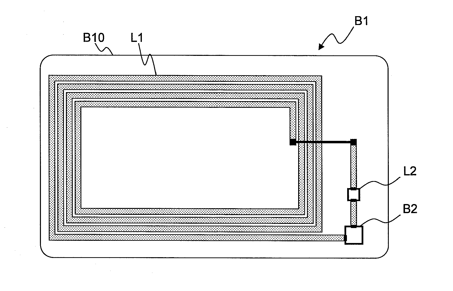
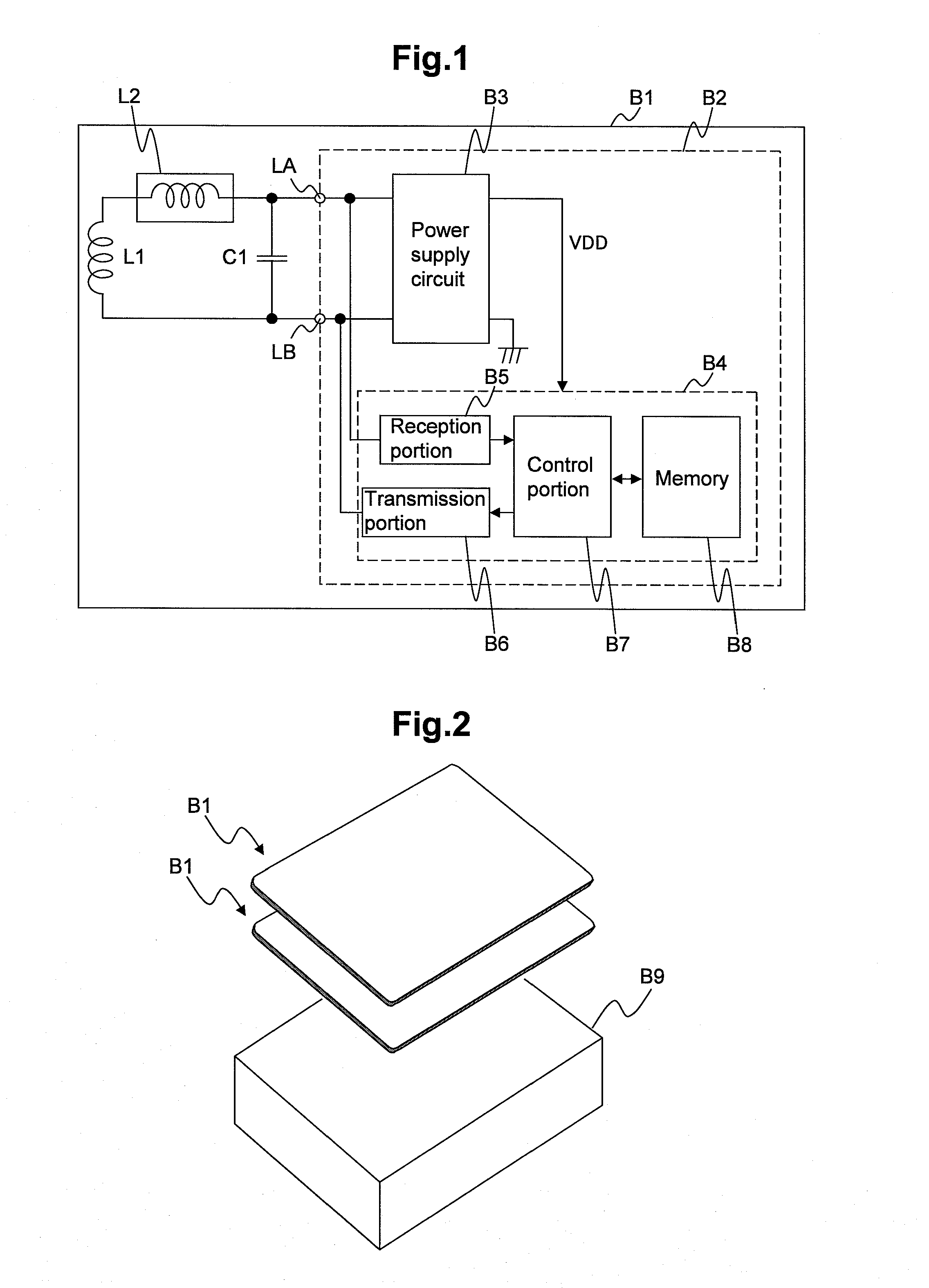
[0049]FIG. 1 illustrates the basic configuration of an IC card as an example of the non-contact electronic device of the invention. In FIG. 1, reference code B1 denotes an IC card; L1 denotes an antenna coil provided in the IC card B1; L2 denotes a coil provided in the IC card B1 and shielded from external electromagnetic waves; C1 denotes a resonance capacitor; and B2 denotes a semiconductor integrated circuit device. The semiconductor integrated circuit device B2 includes: a power supply circuit B3, an internal circuit B4, and antenna terminals LA and LB to which the resonance circuit formed by the antenna coil and the like is coupled. In the example in FIG. 1, the resonance capacitor C1 is provided in the IC card B1. Instead, it may be provided in the semiconductor integrated circuit device B2 or may be divided and provided in the IC card B1 and the semiconductor integrated circuit device B2. In the example in FIG. 1, the coil L2 shielded from electromagnetic waves is comprised o...

second embodiment

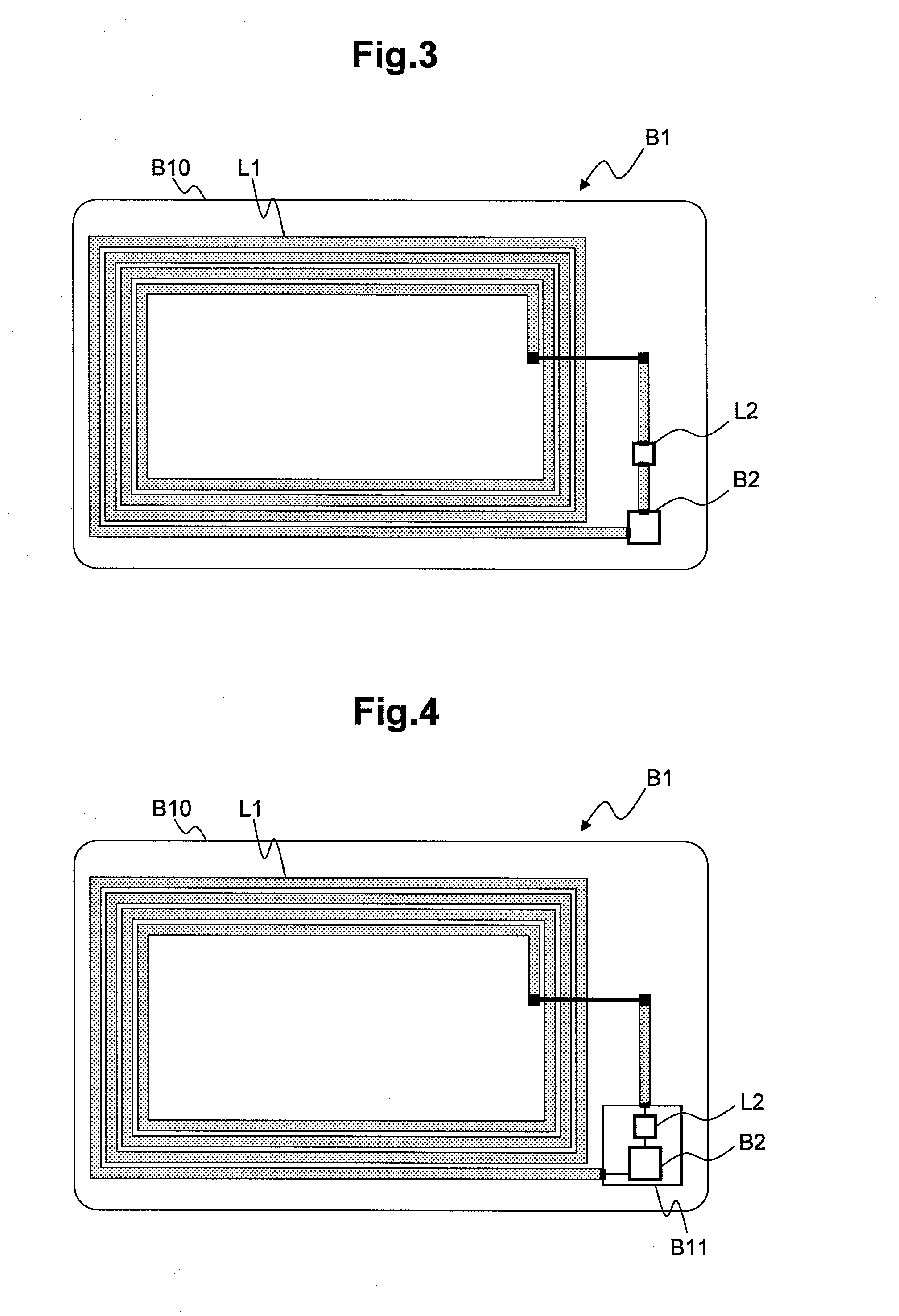
[0067]FIG. 4 illustrates a second example of the IC card. The IC card B1 illustrated in FIG. 4 has its card shape formed by a resin molded printed wiring board. The antenna coil L1 that receives electromagnetic waves from an external reader-writer device is comprised of a spiral coil formed of a wiring of the printed wiring board B10. The semiconductor integrated circuit device B2 and the coil L2 shielded from external electromagnetic waves are each comprised of an IC chip. A resin molded module component B11 in which the semiconductor integrated circuit device B2 and the coil L2 are coupled in series with each other is embedded in the printed wiring board B10 and is coupled to the antenna coil L1.

[0068]In FIG. 4, the resonance capacitor C1 is not shown for the sake of simplification of explanation. However, the resonance capacitor C1 is provided in the printed wiring board B10 forming the IC card B1 or the semiconductor integrated circuit device B2 as required.

[0069]As the result o...

third embodiment

[0075]FIG. 5(A) illustrates the planar configuration of a third example of the IC card and FIG. 5(B) shows a sectional view taken along line X-Y of FIG. 5(A). The IC card B1 illustrated in FIGS. 5(A) and 5(B) has its card shape formed by a resin molded printed wiring board. The antenna coil L1 that receives electromagnetic waves from an external reader-writer device is comprised of a spiral coil formed of a wiring of the printed wiring board B10. The coil L2 shielded from external electromagnetic waves is comprised of: a spiral coil S1 formed of a wiring of the printed wiring board B10; and an electromagnetic wave shielding plate S2 formed of a wiring layer different from the wiring layer forming the spiral coil S1. The semiconductor integrated circuit device B2 is comprised of an IC chip and is coupled to the antenna coil L1 as is coupled in series with the coil L2.

[0076]In FIG. 5, the resonance capacitor C1 is not shown for the sake of simplification of explanation. However, the r...


PUM


Abstract

A non-contact electronic device wherein variation in resonance frequency due to mutual interference between coils provided in individual IC cards can be suppressed and the housing thereof can be easily reduced in thickness is provided. The non-contact electronic device include: a substrate; a first coil for antenna arranged in the substrate; a semiconductor integrated circuit device that is arranged in the substrate and carries out non-contact interface between it and an external source utilizing the first coil; and a second coil comprising a resonance circuit together with the first coil and shielded from electromagnetic waves. Even when multiple non-contact electronic devices are simultaneously used, it is possible to suppress variation in resonance frequency due to mutual interference between the coils provided in individual non-contact electronic devices. Thus stable data communication can be achieved without significant degradation in communication distance regardless of the number of non-contact electronic devices.

Description

FIELD OF THE INVENTION[0001]The present invention relates to non-contact electronic devices that communicate information between them and such devices as reader-writer devices and in particular to a technology effectively applicable mainly to wireless systems in which multiple non-contact electronic devices can be simultaneously used.BACKGROUND OF THE INVENTION[0002]The non-contact electronic devices are provided therein with a semiconductor integrated circuit device and a coil. They exchanges information between, for example, an external reader-writer device and their semiconductor integrated circuit device and implement various functions including: transmitting data held in the relevant non-contact electronic device and holding data transmitted from a reader-writer device. The non-contact electronic devices are represented by IC cards and IC tags. In the description in this document, an IC card will be taken as a representative example and a non-contact electronic device will be h...

Claims


Application Information

Patent Timeline
IPC IPC(8): G06K19/077
CPCG06K19/0723G06K19/0726G06K19/07749H04B5/0075H04B5/0031H04B5/0037H04B5/00H04B5/24H04B5/72H04B5/79
Inventor WATANABE, KAZUKI
Owner RENESAS ELECTRONICS CORP
Learn More