Optical waveguide and coupler apparatus and method of manufacturing the same

a technology which is applied in the field of optical waveguides and couplers, can solve the problems of inability to realize the integration of optical devices with other circuitry, such as memory device circuitry, and the cost of conventional semiconductor wafers in which conventional devices are formed, and achieves the effects of reducing and increasing the cost of optical devices

Active Publication Date: 2011-06-09
SAMSUNG ELECTRONICS CO LTD
View PDF25 Cites 100 Cited by
  • Summary
  • Abstract
  • Description
  • Claims
  • Application Information

AI Technical Summary

Benefits of technology

[0035]In one embodiment, a first sidewall of the core region is a distance d1 from a first sidewall of the trench, a second sidewall of the core region is a distance d2 from a second sidewall of the trench, and the core region has a width w, the width w being a distance between the first sidewall and the second sidewall of the core region, the distances d1 and d2 being selected based on a desired leakage loss in the waveguide due to the substrate. In one embodiment, if both of the distances d1 and d2 are at least 0.27 μm, leakage loss in the waveguide due to the substrate is not mo

Problems solved by technology

The SOI wafers in which conventional devices are formed are considerably more expensive than conventional semiconductor wafers.
Also, because conventional integrated optical devices are formed in SOI substrates, full integration of the optical devic

Method used


Image

  • Optical waveguide and coupler apparatus and method of manufacturing the same
  • Optical waveguide and coupler apparatus and method of manufacturing the same
  • Optical waveguide and coupler apparatus and method of manufacturing the same

Examples


Embodiment Construction

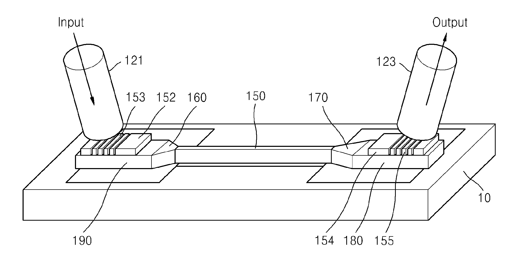
[0137]Various exemplary embodiments will be described more fully hereinafter with reference to the accompanying drawings, in which some exemplary embodiments are shown. The present inventive concept may, however, be embodied in many different for is and should not be construed as limited to the exemplary embodiments set forth herein.

[0138]It will be understood that when an element or layer is referred to as being “on,”“connected to” or “coupled to” another element or layer, it can be directly on, connected or coupled to the other element or layer or intervening elements or layers may be present. In contrast, when an element is referred to as being “directly on,”“directly connected to” or “directly coupled to” another element or layer, there are no intervening elements or layers present. Like numerals refer to like elements throughout. As used herein, the term “and / or” includes any and all combinations of one or more of the associated listed items.

[0139]It will be understood that, al...


PUM


Abstract

Optical waveguide and coupler devices and methods include a trench formed in a bulk semiconductor substrate, for example, a bulk silicon substrate. A bottom cladding layer is formed in the trench, and a core region is formed on the bottom cladding layer. A reflective element, such as a distributed Bragg reflector can be formed under the coupler device and/or the waveguide device. Because the optical devices are integrated in a bulk substrate, they can be readily integrated with other devices on a chip or die in accordance with silicon photonics technology. Specifically, for example, the optical devices can be integrated in a DRAM memory circuit chip die.

Description

RELATED APPLICATIONS[0001]This application relies for priority under 35 U.S.C. 119 on Korean Patent Application numbers 10-2009-0119107, 10-2010-0002390, and 10-2010-0002391, filed in the Korean Intellectual Property Office on Dec. 3, 2009, Jan. 11, 2010, and Jan. 11, 2010, respectively, the entire contents of which applications are incorporated herein by reference.BACKGROUND[0002]1. Field of the Invention[0003]The inventive concept relates to optical devices and methods, and, more specifically, to optical waveguides and couplers used to implement optical communications, and methods of manufacturing the optical waveguides and couplers.[0004]2. Description of the Related Art[0005]Optical devices such as optical fibers, optical waveguides and optical couplers are used for high-speed, low-power communication in various devices and systems. Optical interconnections have been used to achieve large-capacity, high-speed and low-power communication in semiconductor memory devices, modules a...

Claims


Application Information

Patent Timeline
IPC IPC(8): G02B6/42G02B6/02G02B6/34G02B6/26H01L31/12
CPCG02B6/122G02B6/124G02B2006/12104G02B6/34G02B6/4214G02B6/30
Inventor JI, HO-CHULKIM, KI-NAMHYUNG, YONG-WOONA, KYOUNG-WONHA, KYOUNG-HOPARK, YOON-DONGBAE, DAE-LOKBOK, JIN-KWONKANG, PIL-KYUSUH, SUNG-DONGKIM, SEONG-GUSHIN, DONG-JAEJOE, IN-SUNG
Owner SAMSUNG ELECTRONICS CO LTD
Why Eureka
Try Eureka