High Density Opto-Electronic Interconnection Configuration Utilizing Passive Alignment

a passive alignment and interconnection configuration technology, applied in the direction of semiconductor lasers, coupling device connections, instruments, etc., can solve the problem of extremely high cost and achieve the effect of high density and high bandwidth

Active Publication Date: 2019-03-21
AAYUNA INC
View PDF0 Cites 18 Cited by
  • Summary
  • Abstract
  • Description
  • Claims
  • Application Information

AI Technical Summary

Benefits of technology

[0005]The needs remaining in the prior art are addressed by the present invention, which relates to an interconnection configuration for optical communication systems and, more particularly, to a high density, high bandwidth interconnection card utilizing the advantages of 2.5 / 3D packaging to create a backplane connectable arrangement capable of supporting an optical I / O bandwidth of 19.2-76.8 Tb / s in each direction.

Problems solved by technology

However, this improvement has been achieved at an extremely high cost, and often with high power demands and / or the need for relatively large-sized configurations for all of the requisite electrical and optical interconnections.

Method used


Image

  • High Density Opto-Electronic Interconnection Configuration Utilizing Passive Alignment
  • High Density Opto-Electronic Interconnection Configuration Utilizing Passive Alignment
  • High Density Opto-Electronic Interconnection Configuration Utilizing Passive Alignment

Examples


Embodiment Construction

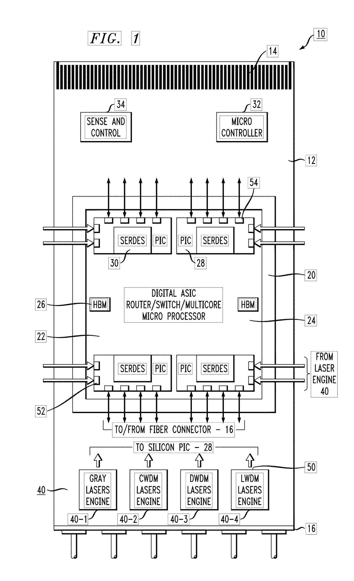
[0058]FIG. 1 is a diagrammatic top view of an exemplary high performance, high speed interconnection configuration 10 formed in accordance with one or more embodiments of the present invention.

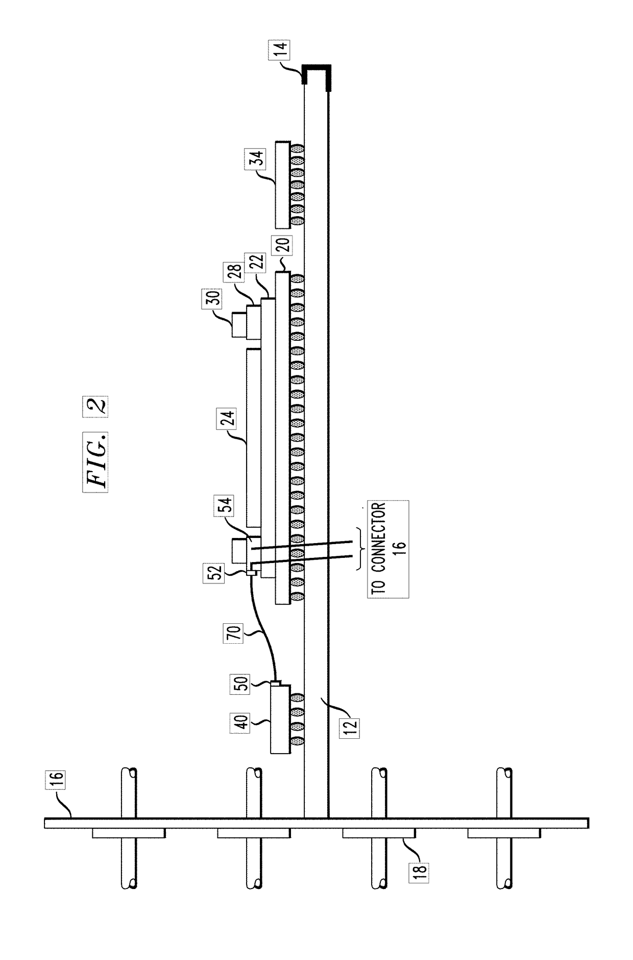
[0059]Configuration 10 takes the form of a backplane-pluggable card formed on a substrate 12 (for example, a PCB, so variously referred to at times hereinafter as “PCB 12”). FIG. 1 is a top view of interconnection configuration 10 (hereinafter referred to as “interconnection card 10”, or simply “card 10”), showing an electrical edge connector 14 formed at a first end termination of substrate 12, and an optical fiber connector 16 formed at a second, opposing end termination of substrate 12. In this particular embodiment of the present invention, the only electrical connection into or out of card 10 is provided via connectors 14; the remainder of the signal paths into and out of card 10 are optical signal paths in the form of optical fibers. FIG. 2 is a side view of configuration 10, particularl...


PUM


Abstract

A high density interconnect arrangement takes the form of a backplane-pluggable card, with electrical connections formed along a single (pluggable) edge and all remaining connections provided via optical fibers. An exemplary interconnect arrangement also includes on-board optical sources and silicon photonic-based circuitry for providing optical transceiver functionality. Passively aligned fiber arrays are utilized to provide I/O connections to external elements, as well as between laser sources and on-board silicon photonics.

Description

CROSS-REFERENCE TO RELATED APPLICATIONS[0001]This application claims the benefit of the following applications: U.S. Provisional Application No. 62 / 560,859, filed Sep. 20, 2017; U.S. Provisional Application No. 62 / 568,013, filed Oct. 4, 2017; U.S. Provisional Application No. 62 / 568,362, filed Oct. 5, 2017, and U.S. Provisional Application No. 62 / 658,668, filed Apr. 17, 2018, the contents of all provisional applications hereby incorporated by reference.TECHNICAL FIELD[0002]The present invention relates to an interconnection configuration for optical communication systems and, more particularly, to a high density, high bandwidth interconnection configuration utilizing the advantages of 2.5 / 3D packaging and silicon photonics to create a backplane connectable arrangement utilizing passive optical alignment between optical fibers and the associated components.BACKGROUND OF THE INVENTION[0003]The next generation high performance opto-electronic systems are known to need about a ten-fold i...

Claims


Application Information

Patent Timeline
Patent Type & Authority Applications(United States)
IPC IPC(8): G02B6/42H01R12/72H01S5/40H01S5/024H01S5/022
CPCG02B6/423H01R12/721G02B6/4216G02B6/4204H01S5/4025H01S5/02469H01S5/02252G02B6/428G02B6/4249G02B6/4268H01S5/02276G02B6/4208G02B6/4212G02B6/4261G02B6/4269G02B6/43H01S5/02326H01S5/02251G02B6/30H01S5/02345
Inventor SHASTRI, KALPENDUSHASTRI, ANUJITPATHAK, SOHAMDAMA, BIPINLEONHARTSBERGER, ALANYELAMARTY, RAO
Owner AAYUNA INC
Why Eureka
Try Eureka