Organic light emitting diode display and method of manufacturing the same

a light-emitting diode and organic technology, applied in the field of organic light-emitting diodes, can solve the problems of inability to smoothly perform subsequent processes, unwanted areas, and organic material layers formed using liquid coating methods, so as to improve the light-emitting characteristic of organic light-emitting elements, reduce contact resistance, and effectively remove organic material layers

Inactive Publication Date: 2011-06-09
SAMSUNG DISPLAY CO LTD
View PDF3 Cites 50 Cited by
  • Summary
  • Abstract
  • Description
  • Claims
  • Application Information

AI Technical Summary

Benefits of technology

[0010]Aspects of the present invention provide an organic light emitting diode (OLED) display and a method of manufacturing the same, having advantages of effectively removing an organic material layer outside of a pixel area while protecting the pixel area, and of improving the light emitting characteristic of an organic light emitting element by minimizing contact resistance between an upper electrode and an upper electrode power source line when connecting them.

Problems solved by technology

However, the organic material layer formed using the liquid coating method is formed not only in the pixel area, but also at unwanted areas, including areas for the scan driver, the data driver, and the contact holes for the upper electrode power source line that are formed outside of the pixel area.
If the organic material layer formed at the outside of the pixel area is not removed, subsequent processes cannot be smoothly performed.

Method used


Image

  • Organic light emitting diode display and method of manufacturing the same
  • Organic light emitting diode display and method of manufacturing the same
  • Organic light emitting diode display and method of manufacturing the same

Examples


Embodiment Construction

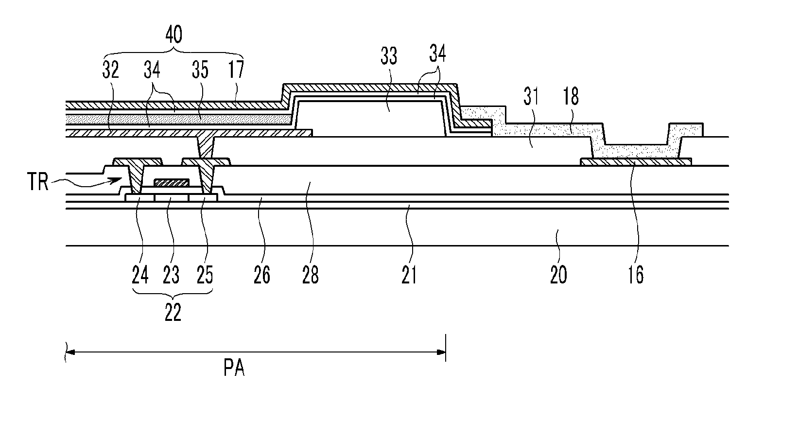
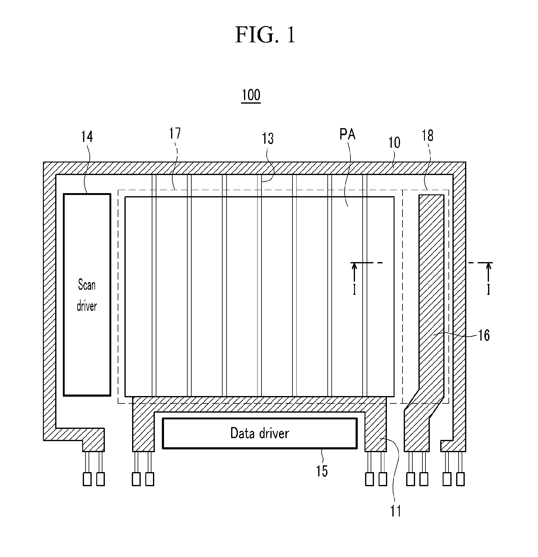
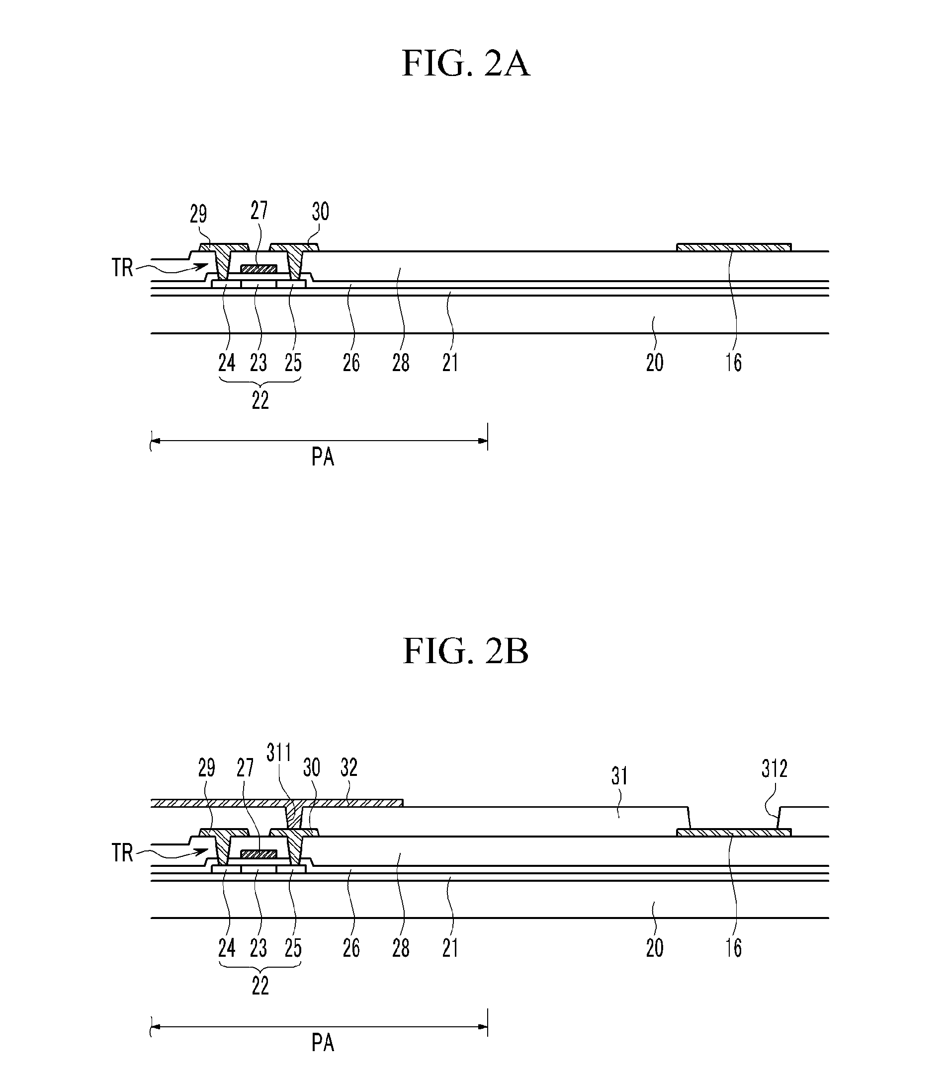
[0053]Reference will now be made in detail to the present embodiments of the present invention, examples of which are illustrated in the accompanying drawings, wherein like reference numerals refer to the like elements throughout. The embodiments are described below in order to explain the present invention by referring to the figures.

[0054]To clarify a description of embodiments of the present invention, parts not related to the description are omitted, and the same reference numbers will be used throughout the drawings to refer to the same or like parts. Further, the size and thickness of each of the elements shown in the drawings are arbitrarily shown for better understanding and ease of description, and the present invention is not limited thereto. For instance, in the drawings, the thickness of layers, films, panels, areas, etc., are exaggerated for clarity. The thickness of the layers and areas are exaggerated in the drawings for better understanding and ease of description. I...


PUM


Abstract

A method of manufacturing an organic light emitting diode (OLED) display includes forming an upper electrode power source line outside of a pixel area over a substrate, forming a lower electrode in the pixel area, forming at least one layer of an organic material layer in the pixel area and areas outside of the pixel area, forming an upper electrode in the pixel area, selectively removing portions of the organic material layer that are exposed outside of the upper electrode, thereby exposing the upper electrode power source line, and coating a conductive material between the upper electrode and the upper electrode power source line in a normal pressure condition such that the conductive material overlaps the upper electrode and the upper electrode power source line, thereby forming a connection portion.

Description

CROSS-REFERENCE TO RELATED APPLICATIONS[0001]This application claims the benefit of Korean Patent Application No. 10-2009-0121361, filed Dec. 8, 2009 in the Korean Intellectual Property Office, the disclosure of which is incorporated herein by reference.BACKGROUND[0002]1. Field[0003]Aspects of the present invention relate to an organic light emitting diode (hereinafter referred to as “OLED”) display. More particularly, aspects of the present invention relate to a method of manufacturing an upper electrode electrically connected to an upper electrode power source line and an OLED display including the upper electrode.[0004]2. Description of the Related Art[0005]An OLED display includes a pixel area including a plurality of pixels. Each of the pixels includes red, green, and blue sub-pixels. An organic light emitting element is formed in each sub-pixel and includes a lower electrode, an organic emission layer, and an upper electrode. The organic emission layer is multilayered, and inc...

Claims


Application Information

Patent Timeline
Patent Type & Authority Applications(United States)
IPC IPC(8): H01L51/52H01L51/56
CPCH01L27/3279H01L2227/323H01L51/56H10K59/1315H10K59/1201H10K71/00H05B33/10
Inventor KANG, JIN-GOOKIM, MU-HYUN
Owner SAMSUNG DISPLAY CO LTD
Why Eureka
Try Eureka