Semiconductor device

a technology of silicon oxide and semiconductors, applied in the direction of semiconductor devices, basic electric elements, electrical equipment, etc., can solve the problems of leakage current, gate insulation layer thinning of silicon oxide, void formation, etc., and achieve the effect of enhancing the reliability and performance of the devi

Active Publication Date: 2011-06-16
UNITED MICROELECTRONICS CORP
View PDF6 Cites 21 Cited by
  • Summary
  • Abstract
  • Description
  • Claims
  • Application Information

AI Technical Summary

Benefits of technology

[0007]Accordingly, the present invention provides a semiconductor device having a v

Problems solved by technology

However, a leakage current occurs when the gate insulation layer of silicon oxide becomes thinner.
However, since the gate structure is shaped as a trapezoid with a bottom wider than a top, when the metal layer

Method used


Image

  • Semiconductor device
  • Semiconductor device
  • Semiconductor device

Examples


Embodiment Construction

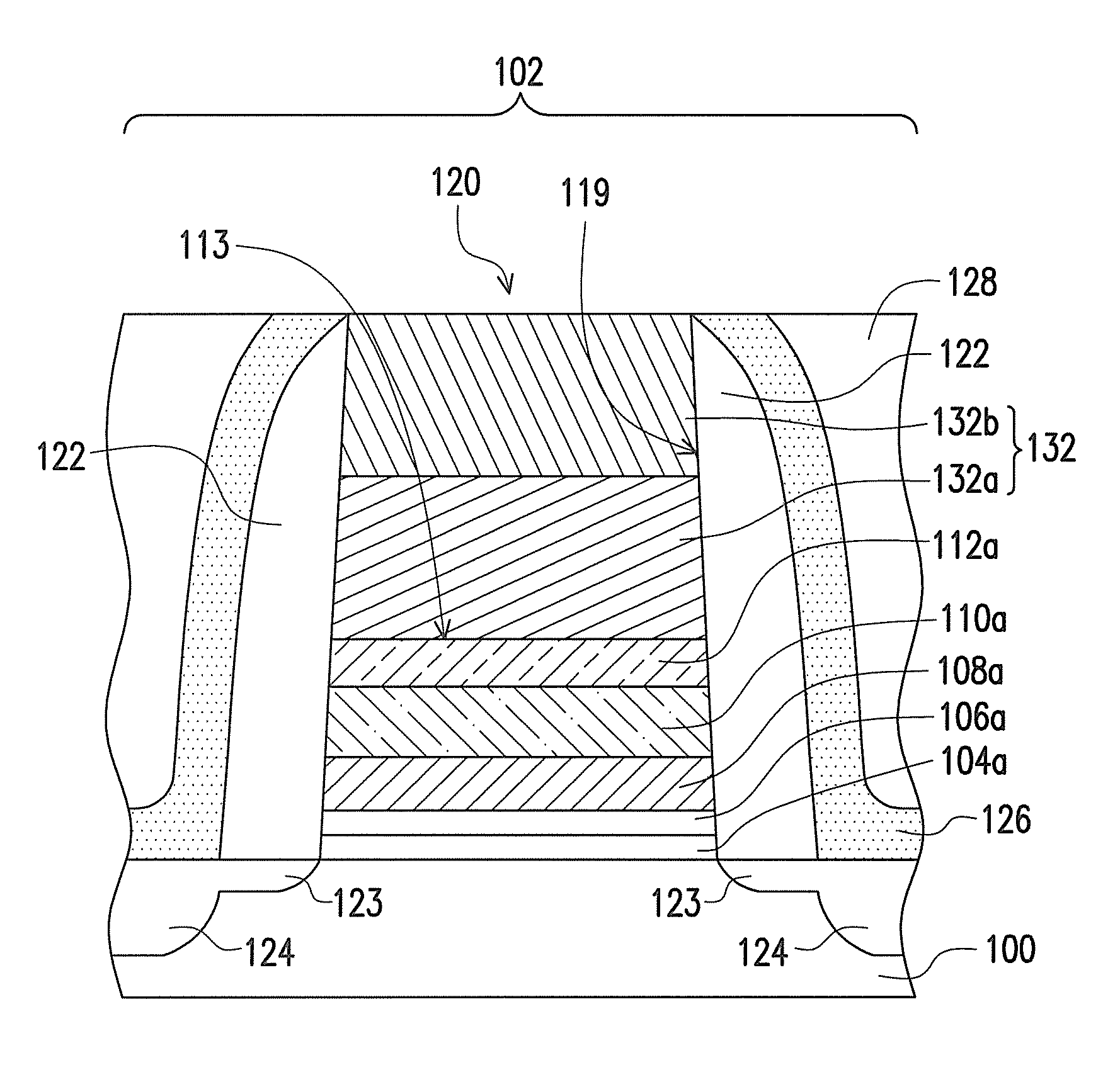
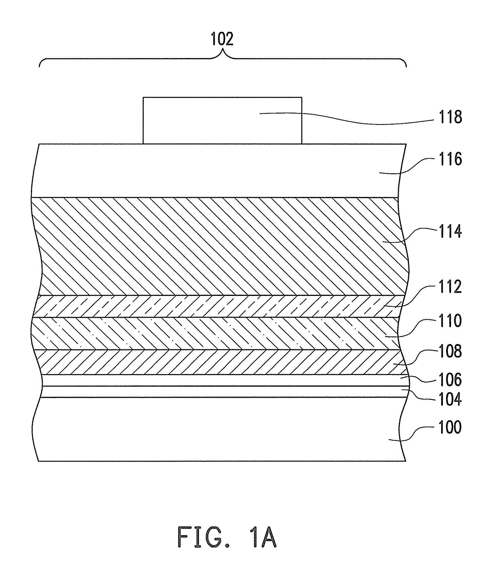
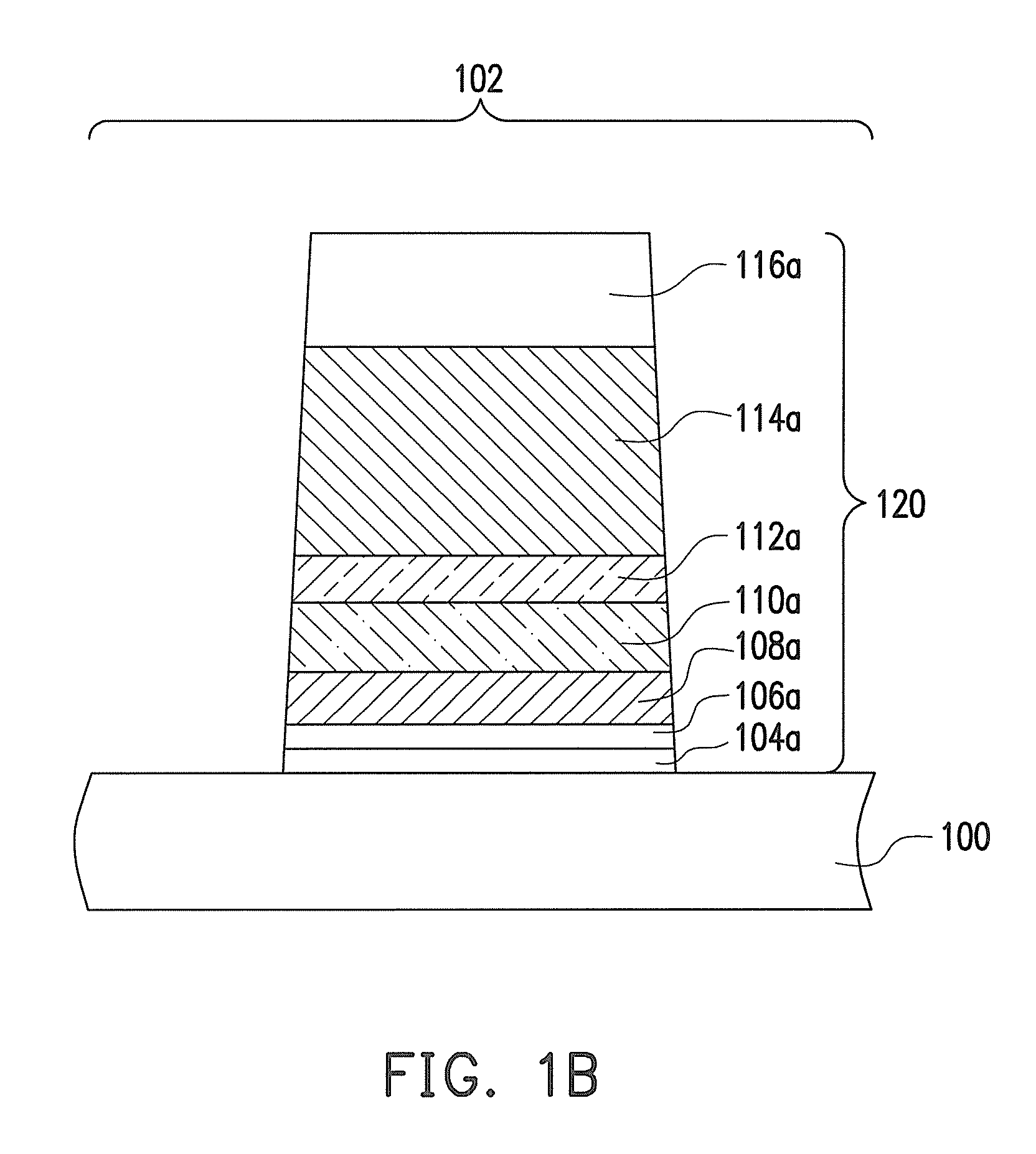
[0033]FIGS. 1A to 1E schematically illustrate, in a cross-sectional view, a method of forming a semiconductor device according to an embodiment of the present invention.

[0034]Referring to FIG. 1A, a substrate 100 is provided. The substrate 100 has a first area 102. The substrate 100 is a silicon substrate, for example. Thereafter, a high-k material layer 106 is formed on the substrate. The high-k material layer 106 includes a material with a dielectric constant greater than 4, such as HfO2, ZrO2, Al2O3, AlN, TiO2, La2O3, Y2O3, Gd2O3, Ta2O5 or a combination thereof, for example. The method of forming the high-k material layer 106 includes performing a CVD process, for example. In an embodiment, an insulation material layer 104 is optionally formed on the substrate 100 before the step of forming the high-k layer 106, so as to increase the adhesion between the high-k layer 106 and the substrate 100. The insulation material layer 104 includes silicon oxide, and the forming method thereo...


PUM


Abstract

A semiconductor device including a substrate, a gate structure, a spacer and source/drain regions is provided. The gate structure is on the substrate, wherein the gate structure includes, from bottom to top, a high-k layer, a work function metal layer, a wetting layer and a metal layer. The spacer is on a sidewall of the gate structure. The source/drain regions are in the substrate beside the gate structure.

Description

CROSS-REFERENCE TO RELATED APPLICATION[0001]This application is a continuation-in-part application of, and claims priority benefits of U.S. patent application Ser. No. 12 / 509,623, filed on Jul. 27, 2009, now pending. The entirety of the above-mentioned patent application is hereby incorporated by reference herein and made a part of this specification.BACKGROUND OF THE INVENTION[0002]1. Field of Invention[0003]The present invention relates to a semiconductor device, and more particularly to a semiconductor device having a void-free metal gate.[0004]2. Description of Related Art[0005]As the dimension of a semiconductor device is getting smaller, the dimension of the gate structure and the thickness of the gate insulation layer are reduced accordingly. However, a leakage current occurs when the gate insulation layer of silicon oxide becomes thinner. To reduce the leakage current, a high dielectric constant (high-k) material is used to replace silicon oxide for forming the gate insulati...

Claims


Application Information

Patent Timeline
IPC IPC(8): H01L29/78
CPCH01L21/28088H01L29/4966H01L29/7843H01L29/66545H01L29/7833H01L29/513
Inventor LIN, CHUN-HSIENHSIEH, CHAO-CHING
Owner UNITED MICROELECTRONICS CORP
Why Eureka
Try Eureka