Semiconductor integrated circuit system and electronic equipment

a technology of integrated circuit system and semiconductor, applied in the direction of generating/distributing signals, pulse techniques, instruments, etc., can solve the problems of increasing test costs, difficult to achieve power supply voltage according to memory cell characteristics, and conventional semiconductor integrated circuit systems, so as to ensure voltages, increase test costs, and facilitate writing and reading

Inactive Publication Date: 2011-06-16
PANASONIC CORP
View PDF8 Cites 10 Cited by
  • Summary
  • Abstract
  • Description
  • Claims
  • Application Information

AI Technical Summary

Benefits of technology

[0027]The semiconductor integrated circuit system may be configured to change the power supply voltage of the memory cell array of the semiconductor memory device according to the output of the monitor circuit in a write operation of the semiconductor memory device, and change a word line voltage of the memory cell array of the semiconductor memory device according to the output of the monitor circuit in a read operation of the semiconductor memory device. In accordance with this configuration, since the power supply voltage and the word line voltage supplied to the semiconductor memory device are changed, according to the output of the monitor circuit during a write operation and a read operation of the semiconductor memory device, it is possible to sufficiently ensure voltages required for the write operation and the read operation of the semiconductor memory device.
[0028]The semiconductor integrated circuit system may further comprises a write assist circuit for changing the power supply voltage of the memory cell array of the semiconductor memory device according to the output of the monitor circuit, in writing of the semiconductor memory device; and a read assist circuit for changing a power supply voltage of a word line driver for driving the word line voltage of the memory cell array of the semiconductor memory device, according to the output of the monitor circuit, in reading of the semiconductor memory device. In accordance with this configuration, the write assist circuit inputs to the memory cell array the voltage regulated according to the output of the monitor circuit as an auxiliary voltage, while the read assist circuit inputs to the memory cell array the voltage regulated according to the output of the monitor circuit as an auxiliary voltage. This makes it possible to easily carry out writing and reading of the semiconductor memory device according to a manufacturing variation.
[0029]An aspect of electronic equipment of the present invention, comprises the semiconductor integrated circuit system having the above configuration, a clock generating circuit for generating a clock signal defining a clock frequency for controlling the semiconductor integrated circuit system; and a controller for changing the clock frequency of the clock signal generated in the clock generating circuit, according to the output of the monitor circuit. In accordance with the electronic equipment having the above configuration, since the voltage output circuit changes the voltage supplied to the semiconductor memory device, according to the characteristics of the memory cells monitored by the monitor circuit, it is possible to supply a voltage which enables the semiconductor memory device to maintain a proper characteristic and operation, to the memory cells constituting the memory cell array of the semiconductor memory device, without increasing a test cost, even when there is a manufacturing variation in the threshold voltages of the transistors of the memory cells or degradation progressing over a long-time use. In addition, since the operational speed of the memory cell changes according to the characteristic change in the memory cell, the controller changes the clock frequency of the clock signal to address the change in the operational speed, and thus the memory cell of the semiconductor memory device can be made operative with an optimal clock frequency. As a result, a higher-speed operation of the electronic equipment is achieved.

Problems solved by technology

However, the conventional semiconductor integrated circuit system has the following problems.
Such a test step brings about an increase in a test cost.
Since a characteristic of the transistors in the memory cell array could be degraded with time, it is difficult to attain a power supply voltage according to a characteristics of the memory cells, merely by setting the voltages based on the characteristics of the transistors obtained in the test step just after the manufacturing.

Method used


Image

  • Semiconductor integrated circuit system and electronic equipment
  • Semiconductor integrated circuit system and electronic equipment
  • Semiconductor integrated circuit system and electronic equipment

Examples


embodiment 1

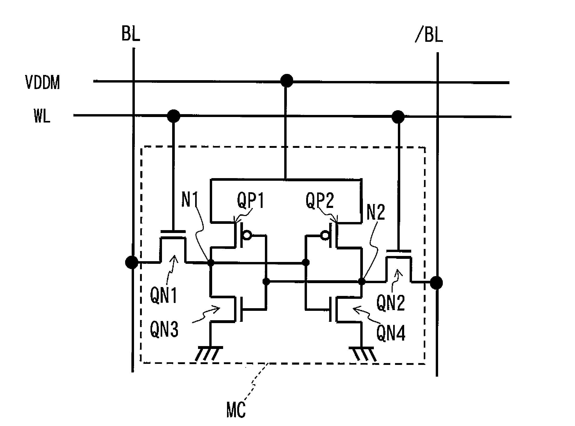
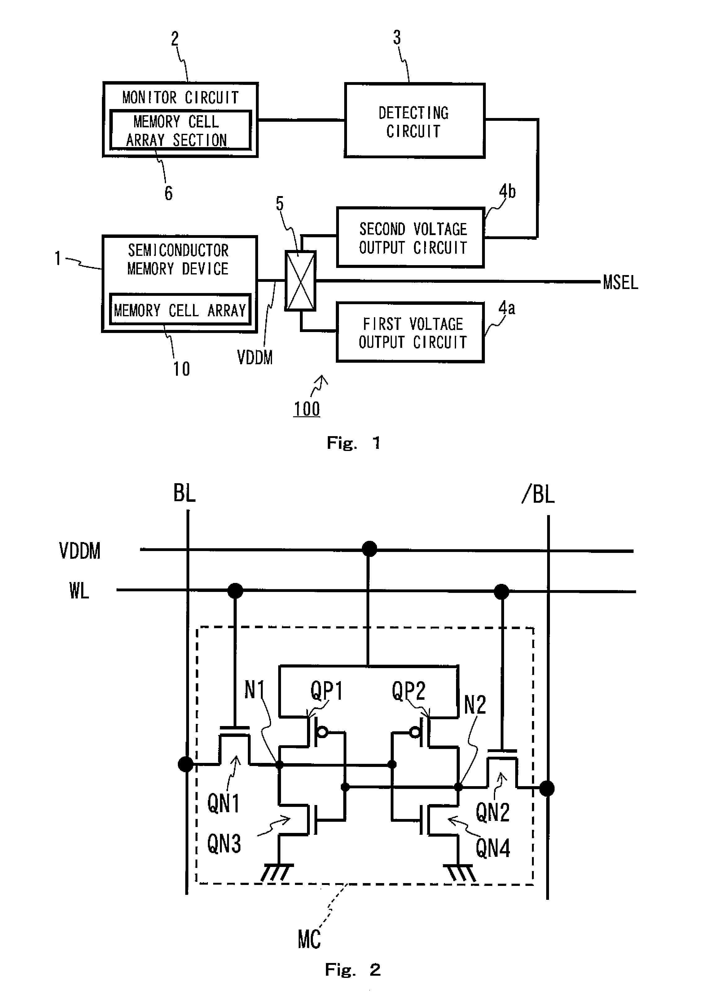
[0060]Initially, a semiconductor integrated circuit system according to Embodiment 1 of the present invention will be described. FIG. 1 is a block diagram showing a schematic configuration of a semiconductor integrated circuit system according to Embodiment 1 of the present invention.

[0061]In this embodiment, as shown in FIG. 1, a semiconductor integrated circuit system 100 includes a semiconductor memory device 1 including a memory cell array 10 having a plurality of memory cells. Further, the semiconductor integrated circuit system 100 includes voltage output circuits each of which outputs a power supply voltage to the memory cell array 10 in the semiconductor memory device 1. In this embodiment, as the voltage output circuits, first and second voltage output circuits 4a, 4b which output voltages different from each other are provided. The first voltage output circuit 4a or the second voltage output circuit 4b is selectively connected to the semiconductor memory device 1 via a swi...

embodiment 2

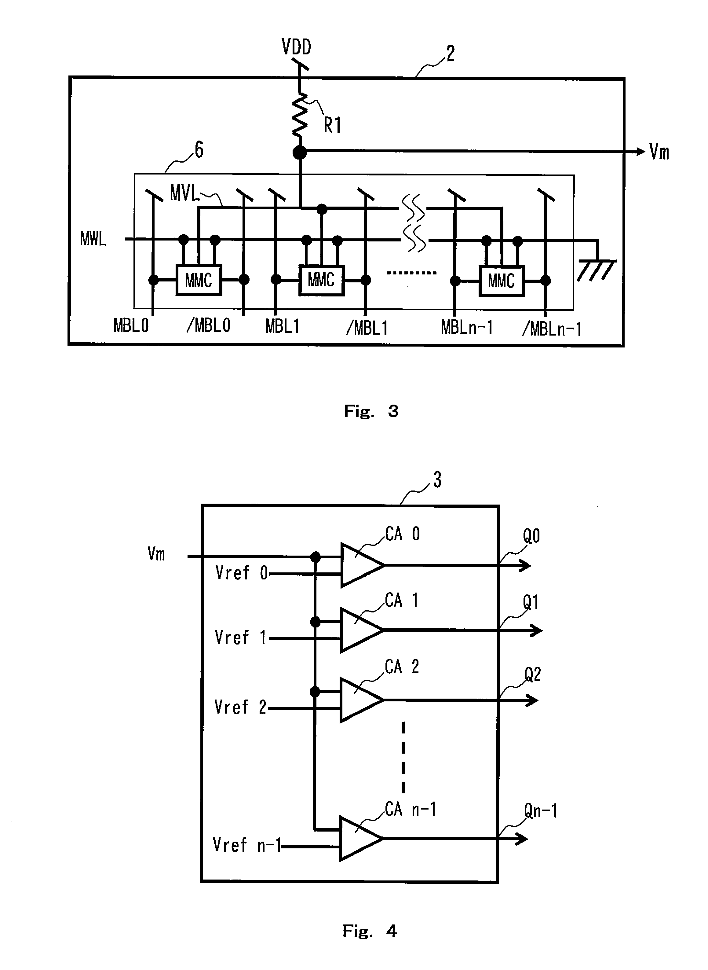
[0085]Subsequently, a semiconductor integrated circuit system according to Embodiment 2 of the present invention will be described. Embodiment 2 is different from Embodiment 1 in that a detecting circuit includes one or more holding circuits for holding output data of one or more comparators CAn. FIG. 6 is a schematic circuit diagram showing a detecting circuit in the semiconductor integrated circuit system according to Embodiment 2 of the present invention. Constituents other than the detecting circuit are identical to those of embodiment 1 and will not be described repetitively.

[0086]The detecting circuit 103 of this embodiment includes one or more comparators CBn (n=0, 1, . . . , n−1) for comparing the output voltage of the monitor circuit 2 to one or more reference voltages Vref (n) (n=0, 1, . . . , n−1). The detecting circuit 103 is configured such that an input terminal of each of the comparators CBn is fed with the output Vm of the monitor circuit 2 and the reference voltage ...

embodiment 3

[0091]Subsequently, a semiconductor integrated circuit system according to Embodiment 3 of the present invention will be described. Embodiment 3 is different from Embodiment 1 in that the power supply switching unit is configured to permit the power supply voltage to be supplied to the first voltage output circuit 4a and inhibit the power supply voltage from being supplied to the second voltage output circuit 4b in a first mode in which the power supply switching unit connects the first voltage output circuit 4a to the semiconductor memory device 1, and permit power supply voltage to be supplied to the second voltage output circuit 4b and inhibit the power supply voltage from being supplied to the first voltage output circuit 4a in the second mode in which the power supply switching unit connects the second voltage output circuit 4b to the semiconductor memory device 1. FIG. 7 is a schematic circuit diagram showing a power supply switching unit in a semiconductor integrated circuit ...


PUM


Abstract

A semiconductor integrated circuit system comprises a semiconductor memory device including a memory cell array having a plurality of memory cells; a monitor circuit for monitoring characteristics of the memory cells; and a voltage output circuit connected to the semiconductor memory device to supply a power supply voltage to the semiconductor memory device; the voltage output circuit being configured to change an output voltage according to an output of the monitor circuit.

Description

CROSS-REFERENCE TO RELATED APPLICATION[0001]This is a continuation application under 35 U.S.C 111(a) of pending prior International application No. PCT / JP2009 / 007057, filed on Dec. 21, 2009. The disclosure of Japanese Patent Application No. 2009-141912 filed on Jun. 15, 2009 including specification, drawings and claims is incorporated here in by reference in its entirety.BACKGROUND OF THE INVENTION[0002]1. Field of the Invention[0003]The present invention relates to a semiconductor integrated circuit system and electronic equipment including a semiconductor memory device.[0004]2. Description of the Related Art[0005]In a semiconductor integrated circuit system, a manufacturing variation in threshold voltages of transistors which are major constituents of the semiconductor integrated circuit system has been increasing because a manufacturing process for miniaturized constituents progresses. Since the variation in the threshold voltages of the transistors causes a problem that a proper...

Claims


Application Information

Patent Timeline
Patent Type & Authority Applications(United States)
IPC IPC(8): G11C7/00G11C5/14G06F1/04
CPCG11C11/41G11C11/417G11C29/02G11C2029/5006G11C29/028G11C29/50G11C2029/0409G11C29/021
Inventor HATANAKA, ICHIROMISUMI, KENJIAIHARA, TOMOYUKISHIRAHAMA, MASANORI
Owner PANASONIC CORP
Why Eureka
Try Eureka