In vacuum optical wafer heater for cryogenic processing

a technology of cryogenic processing and vacuum heating, which is applied in the direction of conveyors, electrical equipment, testing/measurement of semiconductor/solid-state devices, etc., can solve the problems of reducing valuable wafer processing time, affecting manufacturing throughput, and compromising the processing of wafers, so as to prevent unwanted condensation

Active Publication Date: 2011-06-16
VARIAN SEMICON EQUIP ASSOC INC
View PDF5 Cites 354 Cited by
  • Summary
  • Abstract
  • Description
  • Claims
  • Application Information

AI Technical Summary

Benefits of technology

[0009]Exemplary embodiments of the present invention are directed to a vacuum assembly for warming processed substrates above the dew point to prevent unwanted condensation on the processed substrate surfaces. In an exemplary embodiment, such a vacuum assembly includes a processing chamber, a substrate handling robot, and a heater or other radiative energy source. The processing chamber is configured to cryogenically process one or more substrates. The transfer cha

Problems solved by technology

However, processed wafers cannot go from a vacuum environment during implantation to normal atmospheric temperature without creating a coating of condensation on the surface of the waf

Method used


Image

  • In vacuum optical wafer heater for cryogenic processing
  • In vacuum optical wafer heater for cryogenic processing
  • In vacuum optical wafer heater for cryogenic processing

Examples


Embodiment Construction

[0015]The present invention will now he described more fully hereinafter with reference to the accompanying drawings, in which preferred embodiments of the invention are shown. This invention, however, may be embodied in many different forms and should not be construed as limited to the embodiments set forth herein. Rather, these embodiments are provided so that this disclosure will be thorough and complete, and will fully convey the scope of the invention to those skilled in the art. In the drawings, like numbers refer to like elements throughout.

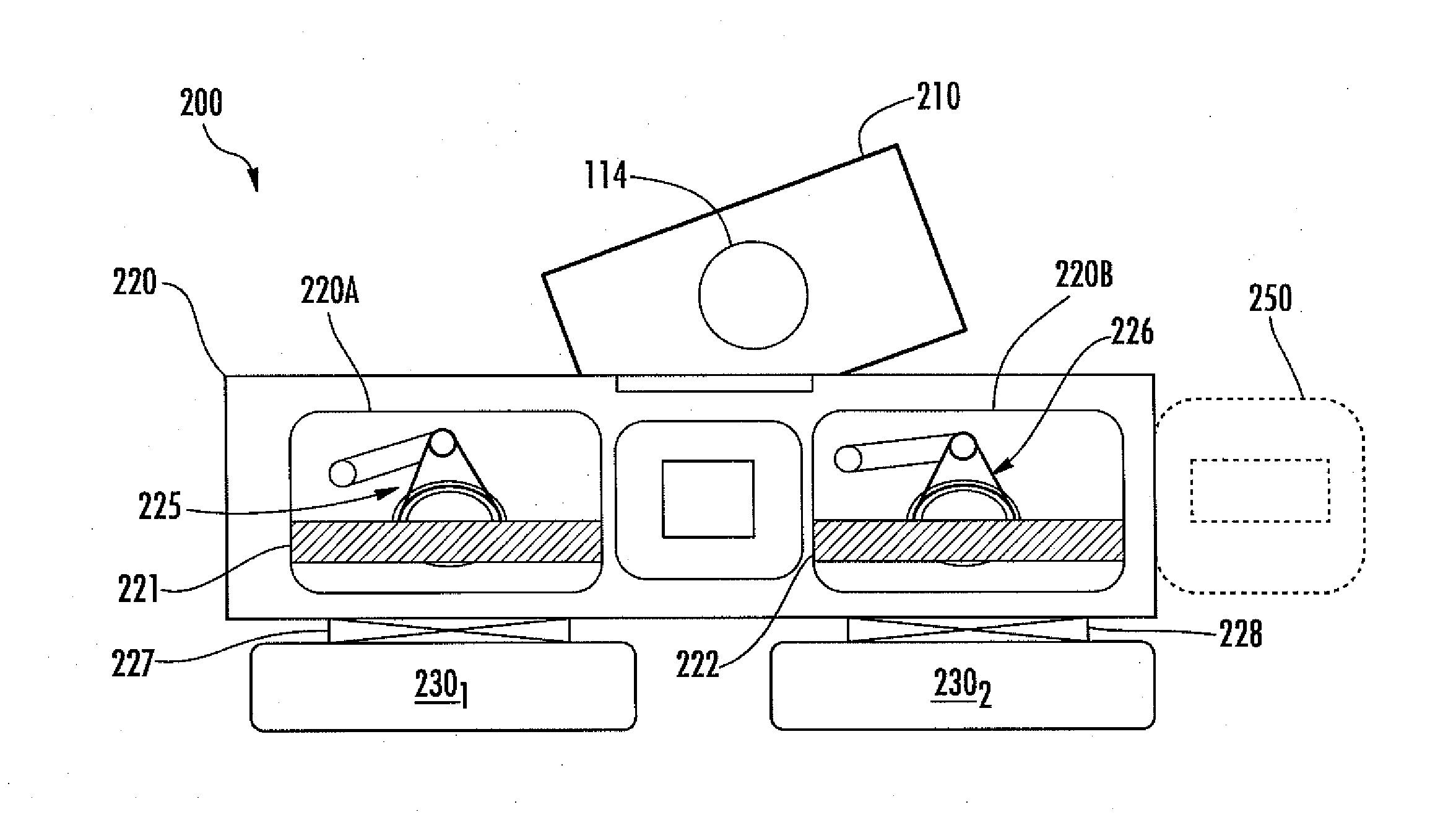
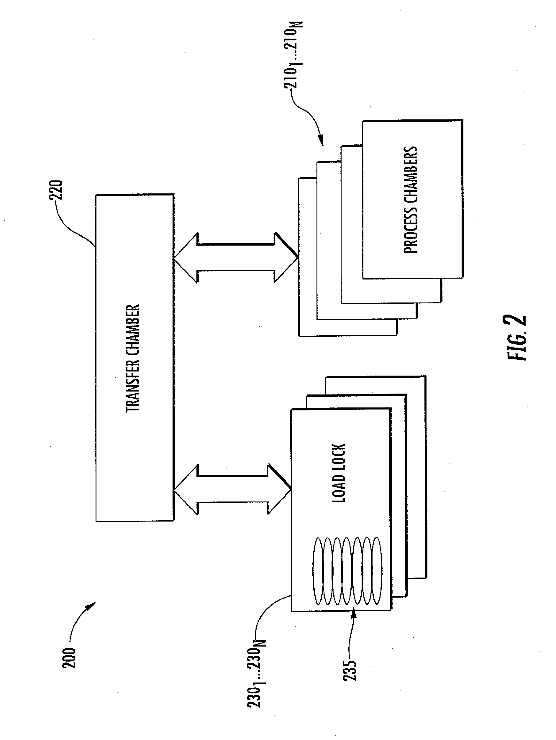
[0016]FIG. 2 is a functional block diagram of a vacuum processing system 200 used in the fabrication of integrated circuits, flat panel displays, etc. The vacuum processing system 200 includes one or more processing chambers 2101 . . . 210N. transfer chamber 220 and one or more loadlock chambers 2301 . . . 230N. Each process chamber houses a support or platen 114 (shown in FIG. 1) which receives a wafer or substrate for processing. Support...


PUM


Abstract

A vacuum assembly used for warming processed substrates above the dew point to prevent unwanted moisture on the processed substrate surfaces as well as reducing negative impact on manufacturing throughput. The vacuum assembly includes a processing chamber, a substrate handling robot, and a heater which may be an optical heater. The processing chamber is configured to cryogenically process one or more substrates. The transfer chamber is connected to the processing chamber and houses the substrate handling robot. The substrate handling robot is configured to displace one or more substrates from the processing chamber to the transfer chamber. The heater is connected to the transfer chamber above the substrate handling robot such that the heater emits energy incident on the substrate when the substrate handling robot displaces the substrate in the transfer chamber.

Description

BACKGROUND OF THE INVENTION[0001]1. Field of the Invention[0002]Embodiments of the invention relate to the field of semiconductor device fabrication. More particularly, the present invention relates to an apparatus for warming processed substrates above the dew point to prevent unwanted moisture on the processed substrate surfaces as well as reducing negative impact on manufacturing throughput.[0003]2. Discussion of Related Art[0004]Ion Implantation is a process used to dope impurity ions into a semiconductor substrate to obtain desired device characteristics. An ion beam is directed from an ion source chamber toward a substrate. The depth of implantation into the substrate is based on the ion implant energy and the mass of the ions generated in the source chamber. One or more ion species may be implanted at different energy and dose levels to obtain desired device structures. In addition, the beam dose (the amount of ions implanted in the substrate) and the beam current (the unifor...

Claims


Application Information

Patent Timeline
IPC IPC(8): H01L21/67H01L21/42H01L21/66
CPCH01L21/67115H01L21/67213H01L21/67196
Inventor FISH, ROGER B.KRAMPERT, JEFFREY E.
Owner VARIAN SEMICON EQUIP ASSOC INC
Why Eureka
Try Eureka