

Microwave anneal of a thin lamina for use in a photovoltaic cell
- Summary
- Abstract
- Description
- Claims
- Application Information
AI Technical Summary
Benefits of technology
Problems solved by technology
Method used
Image

Examples
Embodiment Construction
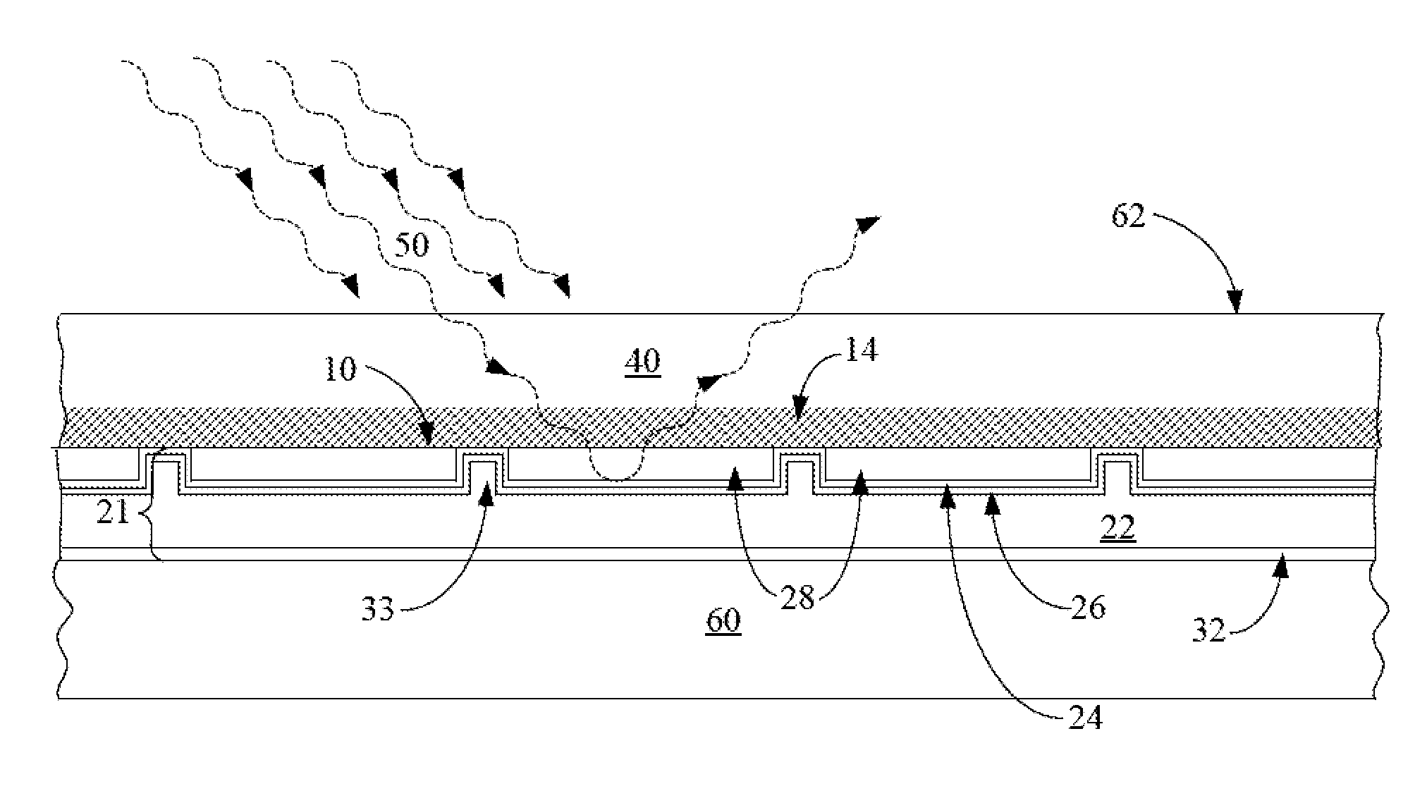
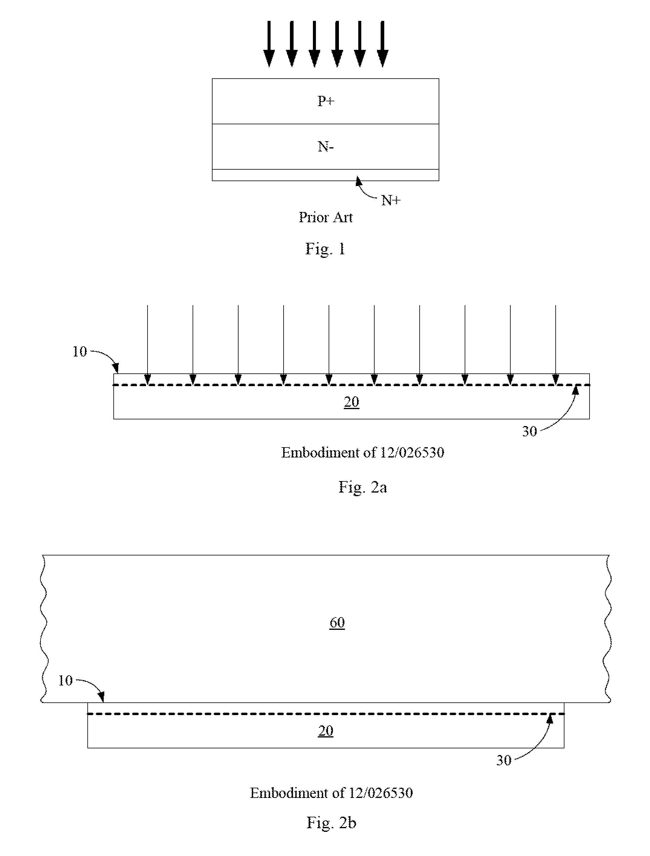
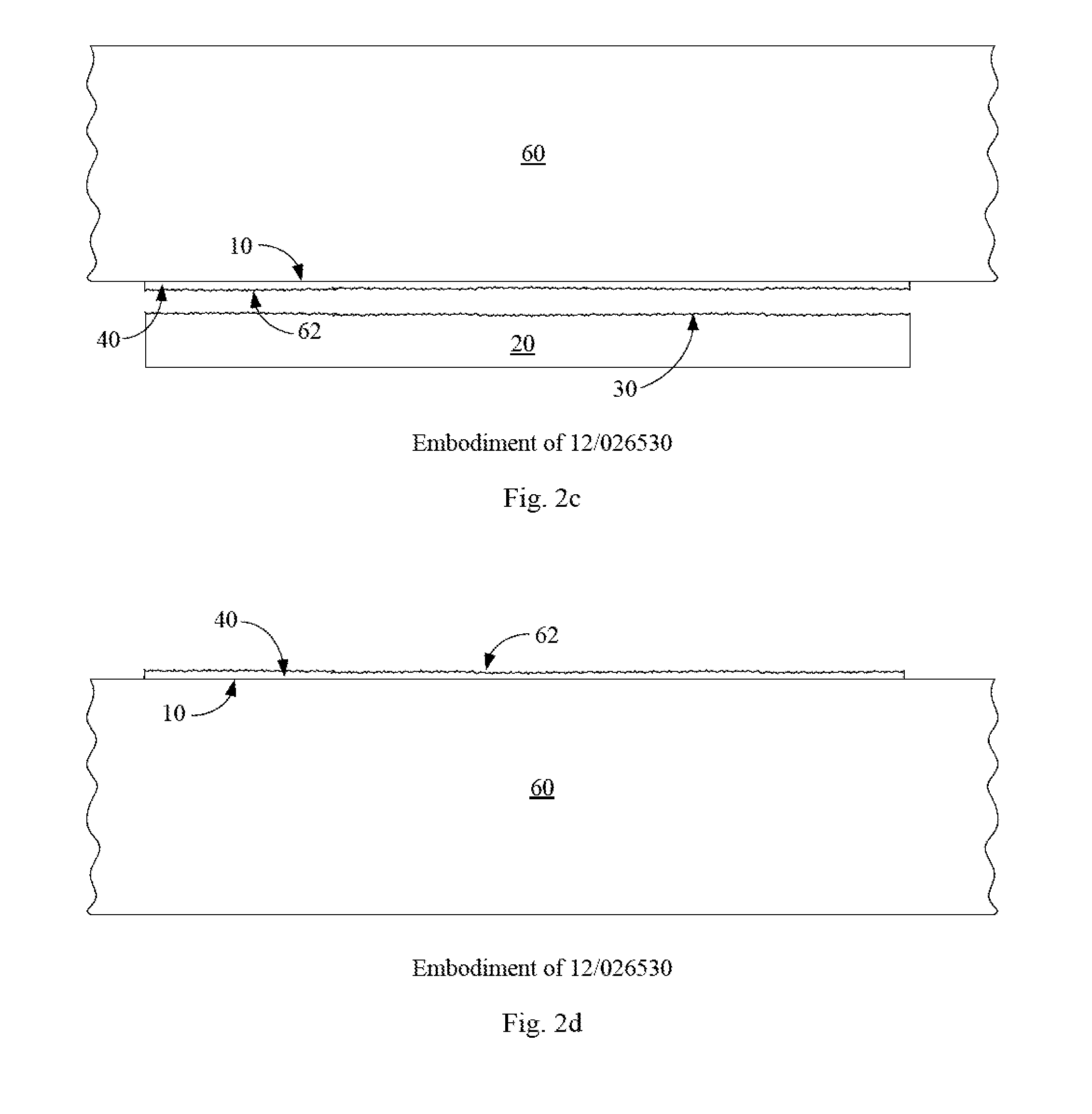
[0003]The present invention is defined by the following claims, and nothing in this section should be taken as a limitation on those claims. In general, the invention is directed to a method to anneal a semiconductor lamina using microwave energy.
[0004]A first aspect of the invention provides for a method to form a photovoltaic cell, the method comprising the steps of: providing a semiconductor lamina bonded to a receiver element, the lamina having a first surface and a second surface opposite the first, the thickness between the first surface and the second surface between about 1.5 microns and about 10 microns, wherein the lamina is bonded to the receiver element at the first surface, with zero, one, or more layers intervening, and the second surface is exposed, and wherein the receiver element has a thickness of at least 80 microns; and annealing the entire thickness of the bonded lamina with microwave energy, wherein the lamina is suitable for use in the photovoltaic cell, and w...
PUM
 Abstract
Description
Claims
Application Information