Image pickup lens, camera module using the same, image pickup lens manufacturing method and camera module manufacturing method

Inactive Publication Date: 2011-06-23
SONY CORP
18 Cites 61 Cited by

AI-Extracted Technical Summary

Problems solved by technology

Therefore, it is difficult to further improve production efficiency and such a method is unsuitable for quantity production.
Therefore, steps such as the optical axis alignment and the like are complicated and cumbersome.
In addition, when the lens portion is formed on one of the surfaces, the lens portion having been formed on the other surface tends to leave residual stress, which causes distortion.
Thus, it is difficult to further improve optical performance.
Therefore, the fixation of the wafer-level wafers 115 becomes complicated and cumbersome because of the steps such as optical axis alignment and the like.
In addition, when the lens portion 113 is formed on one of the ...

Method used

[0059]The camera module 10 configured as above is such that the first glass lens substrate 14 is formed with the first and second resin layers 15a, 15b on both the sides thereof and the first and second spacers 23 and 24 are formed integrally with the first and second lens portions 16 and 17, respectively. As described later, the first and second lens portions 16, 17 and the first and second spacers 23, 24 are simultaneously formed by setting the first and second glass lens substrates 14, 18 in a molding device 30, pouring a resin material such as a thermosetting resin into the molding device and curing it. This eliminates adjusting work such as optical axis alignment for the first and second lens portions 16, 17, which can improve production efficiency. Also the first spacer 23 is formed simultaneously with the first and second lens portions 16, 17; therefore, assembly becomes more easily than in the case where the spacer is a separate member as in a traditional way. The first and second lens portions 16, 17 are simultaneously formed by injection molding; therefore, it is possible to prevent the occurrence of distortion at the first lens portion when the second lens portion is formed after the formation of the first lens portion as in a traditional way. Thus, optical characteristics can be enhanced. Incidentally, such an effect applies to the second image pickup lens 12.
[0061]Referring to FIG. 5, the molding device 30 used to manufacture the first image pickup lens 11 includes a first mold 31 used to form a first lens portion 16 side and a second mold 32 used to form a second lens portion 17 side. The molding device 30 is installed e.g. in a clean room 46 so that foreign matter is prevented from entering the first image pickup lens 11, making it possible to manufacture the first image pickup lens 11 with a high degree of optical accuracy.
[0077]As illustrated in FIG. 9, in the method of manufacturing the camera module 10 described above, the first lens portions 16 and second lens portions 17 of the first image pickup lens wafer 39 are simultaneously formed. Therefore, a step such as optical axis adjustment or the like between the first lens portion 16 and the second lens portion is not necessary. The third lens portions 21 and fourth lens portions 22 of the second image pickup lens wafer 47 are simultaneously formed. Therefore, a step such as optical axis adjustment or the like between the third lens portion 21 and the fourth lens portion 22 are not necessary. Thus, the step of manufacturing the first image pickup lens wafer 39 and the second image pickup lens wafer 47 is simplified to achieve an improvement in production efficiency. The first lens portion and the second lens portion 17 are simul...

Benefits of technology

[0017]According to the present invention, the spacer is formed integrally with the lens portion on any one of the surfaces of the substrate; therefore, even when the image pickup lenses are stacked one on another, it is not necessary to use a spacer as a separate member. In addition, even if the lens portions are provided on both the respective surfac...

Abstract

An image pickup lens is provided that includes a substrate; resin layers formed on both respective opposite surfaces of the substrate; a lens portion formed on at least any one of the surfaces of the substrate; and a spacer formed on at least any one of the surfaces of the substrate at an area surrounding the lens portion.

Application Domain

Technology Topic

Image

  • Image pickup lens, camera module using the same, image pickup lens manufacturing method and camera module manufacturing method
  • Image pickup lens, camera module using the same, image pickup lens manufacturing method and camera module manufacturing method
  • Image pickup lens, camera module using the same, image pickup lens manufacturing method and camera module manufacturing method

Examples

  • Experimental program(1)

Example

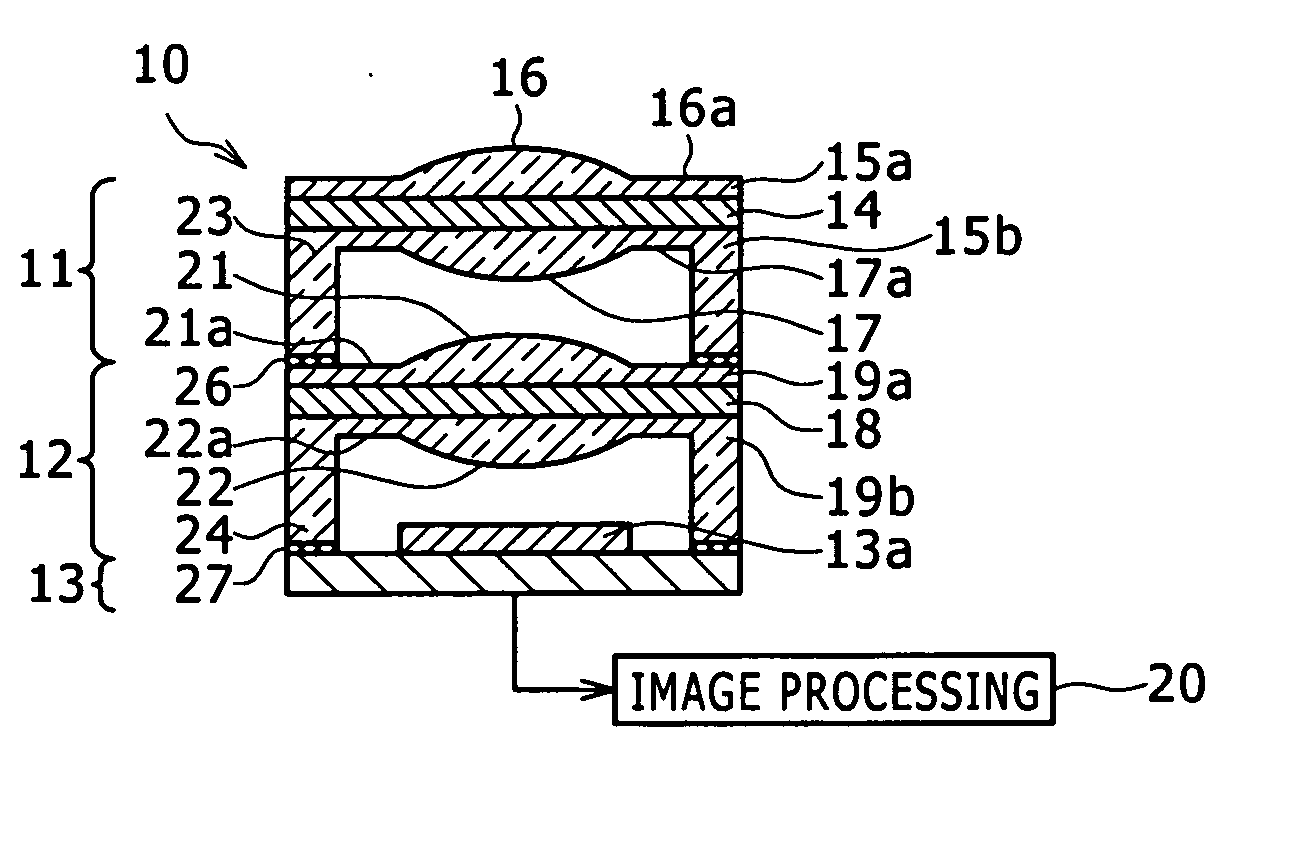
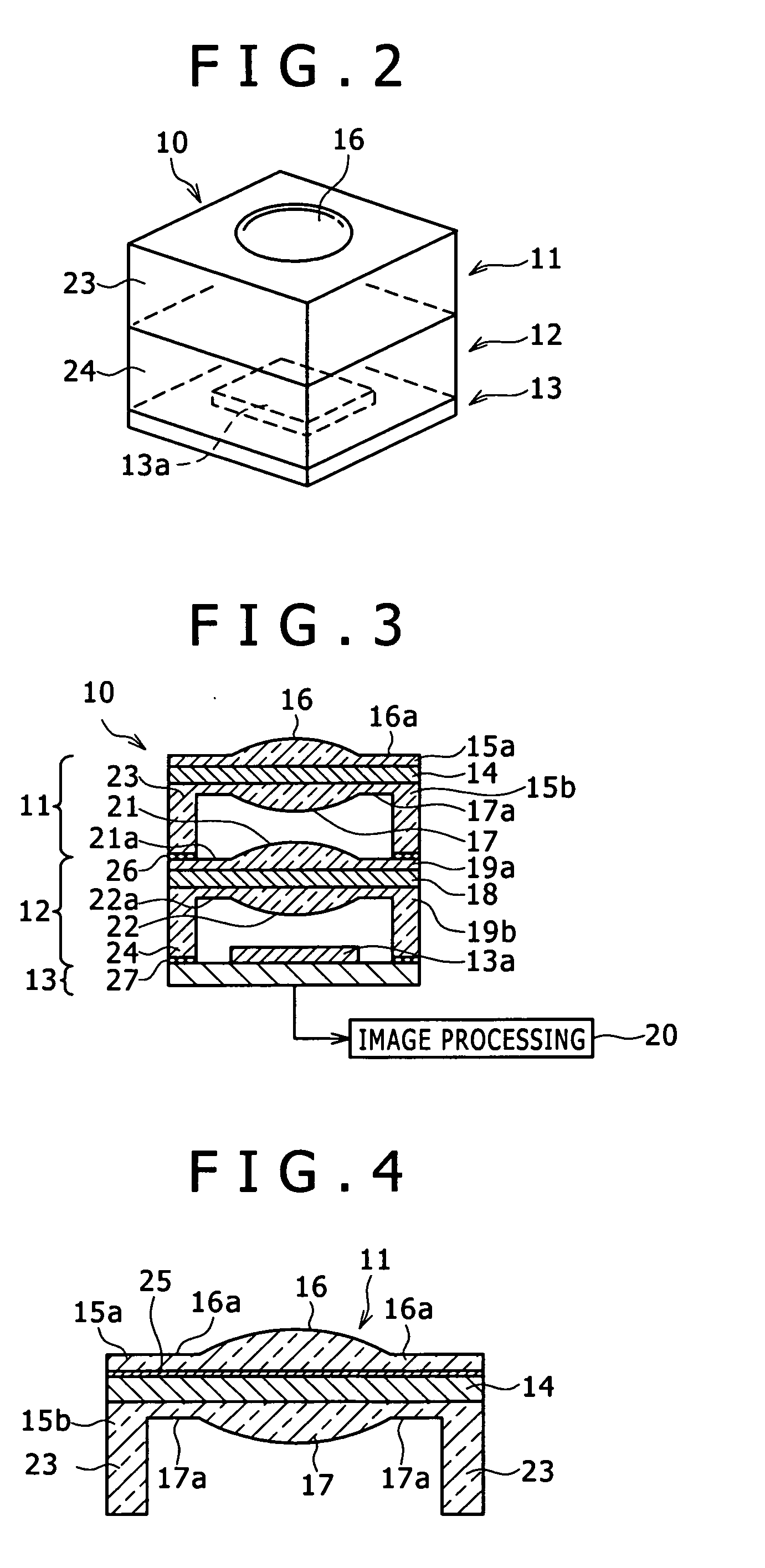
[0038]A description will hereinafter be described of camera modules according to embodiments of the present invention with reference to the drawings. Incidentally, the embodiment of the invention is below described in the following order.
[0039](1) A description of a mobile phone
[0040](2) A description of a camera module
[0041](3) A description of a camera module manufacturing method
[0042](4) Modifications [0043] (4-1) A modification of a glass lens substrate [0044] (4-2) A modification of an image pickup lens [0045] (4-3) A modification of a spacer [0046] (4-4) Other modifications
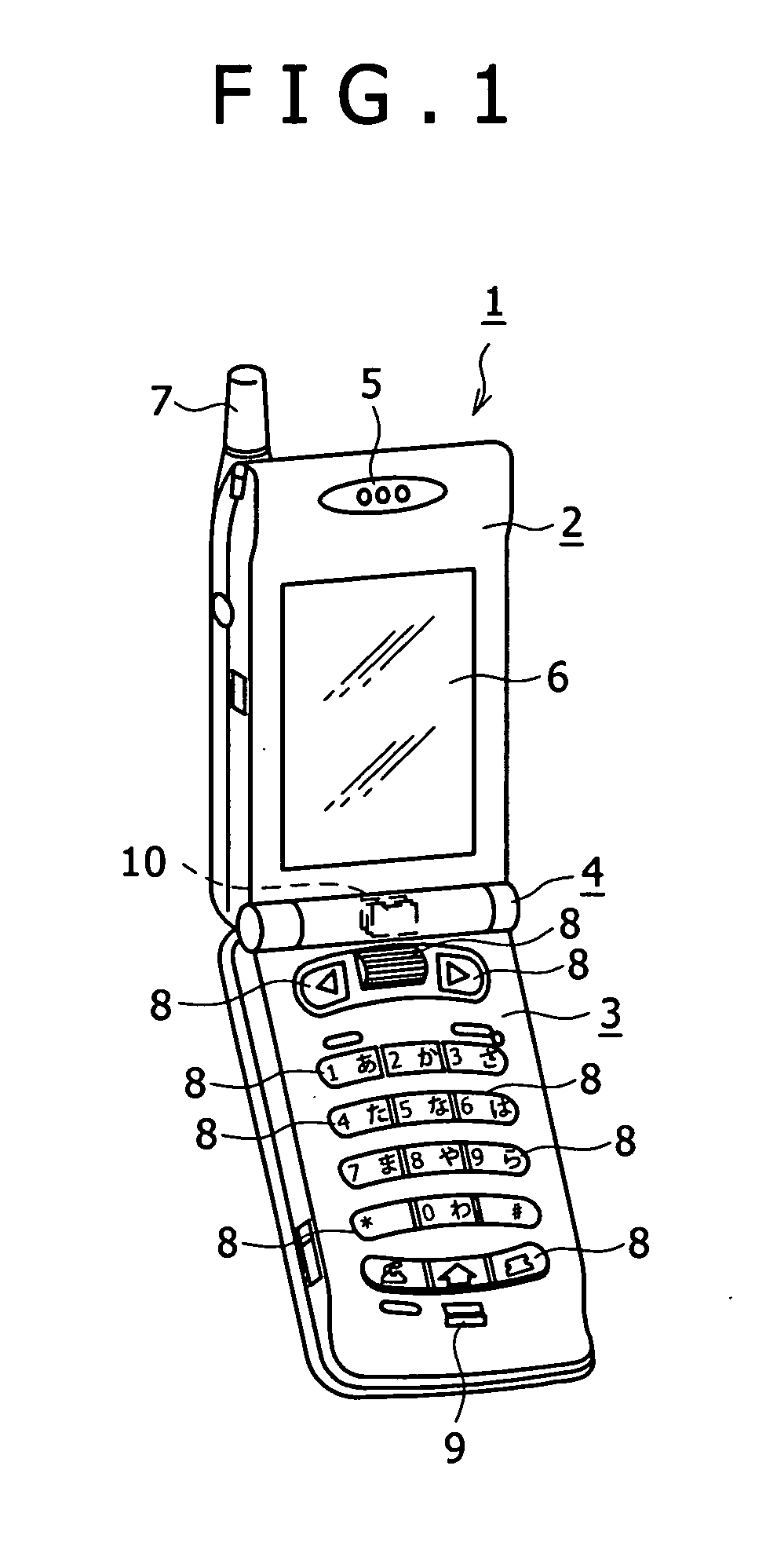
(1) A Description of a Mobile Phone
[0047]Referring to FIG. 1, a mobile phone 1 on which a cameral module according to an embodiment of the present invention is mounted is such that a first casing 2 and a second casing 3 are coupled to each other in a foldable manner via a hinge portion 4. The first casing 2 is provided with a speaker 5, a display portion 6 and an antenna 7. The antenna 7 is telescopic. The second casing 3 is provided with various operating portions 8 including push buttons and a rotary dial and with a microphone 9. A camera module 10 is assembled in the hinge portion 4. A predetermined push button of the operating portions 8 functions as an operating portion 8 to pick up images. This operating portion 8 is operatively pushed to operate the camera module 10, thereby allowing for picking up images. In short, this mobile phone 1 is an electronic device or information-processing device functioning as also an image pickup device.
[0048]Incidentally, the camera module 10 may be located in the first casing 2 or second casing 3 as well as in the hinge portion 4. A plurality of the camera modules 10 may be mounted on the single mobile phone 1.
(2) A Description of a Camera Module
[0049]Referring to FIGS. 2 and 3, the camera module 10 embodying the present invention is configured such that a first image pickup lens 11, a second image pickup lens 12 and an image pickup substrate 13 provided with an image pickup device 13a are stacked one on another.
[0050]Referring to FIGS. 2 to 4, the first image pickup lens 11 is such that a first resin layer 15a is formed on one of surfaces of a first glass lens substrate 14 and a second resin layer 15b is formed on the other surface. The first glass lens substrate 14 is made of e.g. a parallel flat plate and has optical transparency. The first resin layer 15a is formed with a first lens portion 16 formed e.g. in a convex shape and the second resin layer 15b is formed with a second lens portion 17 formed e.g. in a convex shape. The periphery of the first lens portion 16 is formed as a flat portion 16a and that of the second lens portion 17 is formed as a flat portion 17a. In short, the first glass lens substrate 14 is formed with the first and second resin layers 15a, 15b on both the surfaces thereof.
[0051]The second image pickup lens 12 is such that a third resin layer 19a is formed on one of surfaces of a second glass lens substrate 18 and a fourth resin layer 19b is formed on the other surface. The second glass lens substrate 18 is made of e.g. a parallel flat plate and has optical transparency. The third resin layer 19a is formed with a third lens portion formed e.g. in a convex shape and the fourth resin layer 19b is formed with a fourth lens portion 22 formed e.g. in a convex shape. The periphery of the third lens portion 21 is formed as a flat portion 21a and that of the fourth lens portion 22 is formed as a flat portion 22a. In short, the second glass lens substrate 18 is formed with the third and fourth resin layers 19a, 19b on both the surfaces thereof.
[0052]Incidentally, the first through fourth lens portions 16, 17, 21, 22 may each be formed not only in the convex shape but in a concave shape. The camera module 10 may fully be formed to have flat portions each formed of a resin layer without the first through fourth lens portions 16, 17, 21, 22 in accordance with the use application thereof. The number of stages of the image pickup lens is not limited to two as described above but may be one or three or more.
[0053]On the first glass lens substrate 14, the second resin layer 15b is formed with a first spacer 23 on the periphery of the second lens portion 17. In addition, on the second glass lens substrate 18, the fourth resin layer 19b is formed with a second spacer 24 on the periphery of the fourth lens portion 22. The first spacer 23, of the second resin layer 15b, integral with the second lens portion 17 via the flat portion 17a on the periphery of the second lens portion is formed to project from the other surface of the first glass lens substrate 14 to define a given interval between the third lens portion 21 and the second lens portion 17. In addition, the second spacer 24, of the fourth resin layer 19b, integral with the fourth lens portion 22 via the flat portion 22a on the periphery of the fourth lens portion 22 is formed to project from the other surface of the second glass lens substrate 18 to define a given interval between the image pickup substrate 13 and the fourth resin layer 19b. The first spacer 23 is formed to surround the first glass lens substrate shaped in a general rectangle. The second spacer 24 is formed to surround the second glass lens substrate 18 shaped in a general rectangle. In this way, a light-shield space is defined between the second lens portion 17 and the third lens portion 21 and between the fourth lens portion 22 and the image pickup device 13a to prevent the entrance of outsight light into an optical path.
[0054]The first image pickup lens 11 is formed with an infrared reflective film 25 between the first glass lens substrate 14 and the first resin layer 15a. The infrared reflective film 25 is formed by depositing an infrared reflective material on one of the surfaces of the first glass lens substrate 14 by sputtering, deposition or the like. Incidentally, the infrared reflective film 25 may not be provided. The first image pickup lens 11 can omit the infrared reflective film 25 by dispersing an infrared absorption agent into the resin material of the first resin layer 15a.
[0055]The image pickup substrate 13 is a semiconductor substrate such as a silicon substrate or the like and formed with the image pickup device 13a. Incidentally, the image pickup substrate 13 may be an organic resin substrate made of a glass epoxy resin, polyimide or the like.
[0056]Next, the first image pickup lens 11 is bonded to the second image pickup lens 12 at a portion surrounding the third lens portion 21 of the second image pickup lens 12 with a first adhesive 26 coated on the end face of the first spacer 23. The second image pickup lens 12 is bonded to the image pickup substrate 13 at a portion surrounding the image pickup device 13a of the image pickup substrate 13 with a second adhesive 27 coated on the end face of the second spacer 24.
[0057]Incidentally, the first spacer 23 is here bonded to the third resin layer 19a at a portion surrounding the third lens portion 21; however, the first spacer 23 may directly be bonded to the second glass lens substrate 18 not formed with the third resin layer as described later.
[0058]In the camera module 10 configured as described above, imaging light having passed through the first through fourth lens portions 16, 17, 21 and 22 is received by the image pickup device 13a. Incidentally, in the camera module 10, the first image pickup lens 11 and the second image pickup lens 12 are stationary, that is, are not movable unlike a focus lens or a zoom lens. Therefore, an image-processing section 20 electrically connected to the image pickup device 13a performs image processing, i.e., focusing processing and/or zooming processing, on the image date obtained by the image pickup device 13a, thereby providing image data desired by a user.
[0059]The camera module 10 configured as above is such that the first glass lens substrate 14 is formed with the first and second resin layers 15a, 15b on both the sides thereof and the first and second spacers 23 and 24 are formed integrally with the first and second lens portions 16 and 17, respectively. As described later, the first and second lens portions 16, 17 and the first and second spacers 23, 24 are simultaneously formed by setting the first and second glass lens substrates 14, 18 in a molding device 30, pouring a resin material such as a thermosetting resin into the molding device and curing it. This eliminates adjusting work such as optical axis alignment for the first and second lens portions 16, 17, which can improve production efficiency. Also the first spacer 23 is formed simultaneously with the first and second lens portions 16, 17; therefore, assembly becomes more easily than in the case where the spacer is a separate member as in a traditional way. The first and second lens portions 16, 17 are simultaneously formed by injection molding; therefore, it is possible to prevent the occurrence of distortion at the first lens portion when the second lens portion is formed after the formation of the first lens portion as in a traditional way. Thus, optical characteristics can be enhanced. Incidentally, such an effect applies to the second image pickup lens 12.
(3) A Description of a Camera Module Manufacturing Method
[0060]A description is next given of a method of manufacturing the first image pickup lens 11. Incidentally, the detailed description of a method of manufacturing the second image pickup lens 12 is omitted because the method of manufacturing the second image pickup lens 12 is the same as the method of manufacturing the first image pickup lens 11.
[0061]Referring to FIG. 5, the molding device 30 used to manufacture the first image pickup lens 11 includes a first mold 31 used to form a first lens portion 16 side and a second mold 32 used to form a second lens portion 17 side. The molding device 30 is installed e.g. in a clean room 46 so that foreign matter is prevented from entering the first image pickup lens 11, making it possible to manufacture the first image pickup lens 11 with a high degree of optical accuracy.
[0062]In the first mold 31, first lens portion forming portions 33 forming the first lens portions 16 and flat portion forming portions 34 forming flat portions 16a on the peripheries of the first lens portions 16 are continuously formed. The first mold 31 is formed at an end with a substrate support portion 35 supporting the first glass lens substrate 14.
[0063]In the second mold 32, second lens portion forming portions 36 forming the second lens portions 17, flat portion forming portions 37 forming the flat portions 17a surrounding the second lens portions 17, and the first spacer forming portions 38 forming the first spacers 23 are continuously formed. Further, the second mold 32 is formed at an end with a second substrate support portion 40, which supports the first glass lens substrate 14 in cooperation with the first substrate support portion 35. The first substrate support portion 35 and the second substrate support portion 40 serve as a substrate holding portion to hold the first glass lens substrate 14 with the first mold 31 and the second mold 32 clamped together.
[0064]Referring to FIG. 6, the first mold 31 and the second mold 32 are clamped together to define a cavity 41, which is adapted to form a first image pickup lens wafer 39 formed with a large number of the first image pickup lenses 11 on a surface.
[0065]Similarly to the second image pickup lens 12, the first image pickup lens 11 uses a thermosetting resin. Therefore, similarly to the common mold, the first and second molds 31, 32 can be formed with the forming surface of the cavity 41 by cutting metal. Examples of the thermosetting resin used herein include acrylic, epoxy, and silicon. The thermosetting resin may be of a single-liquid type or a two-liquid type (epoxy or silicon) of a base resin and a setting agent. An example of the thermosetting resin of the two-liquid type includes Toray Corning OE-6636.
[0066]Incidentally, if an ultraviolet curable resin is used as the resin material, the first mold 31 and the second mold 32 need to have optical transparency; therefore, they are made of e.g. glass or the like.
[0067]In the molding device 30 configured as above, the first glass lens substrate 14 is mounted on any one of the respective substrate support portions 35, 40 of the first and second molds 31, 32. Thereafter, the first and second molds 32, 33 are brought close to each other and clamped together. Incidentally, in the embodiment, the first glass lens substrate 14 is first mounted on the second substrate support portion 40 of the second mold 33.
[0068]After the mold clamping is performed to define the cavity 41 inside the first and second molds 31, 32, as shown in FIG. 6, a molten thermosetting resin 45 is injected from a nozzle 42 into the cavity 41. At the same time, the clean room 46 is deaerated from a deaerating port 43 connected to a vacuum pump. In other words, since the molten thermosetting resin 45 may contain bubbles because of low viscosity, defoaming is performed via an opening portion 40a opened in the upper portion of the molding device.
[0069]Referring to FIG. 7, the first mold 31 and/or the second mold 32 are next heated by a heating device 44 to perform thermosetting processing on the thermosetting resin 45.
[0070]After the thermosetting resin 45 in the cavity 41 is set, the heating is stopped. Referring to FIG. 8, the first mold 31 and the second mold 32 are next opened from each other and the first image pickup lens wafer 39 is taken out from any one of the first mold 31 and the second mold 32 by e.g. an ejecting mechanism. In this way, as illustrated in FIGS. 9 and 10, the first image pickup lens wafer 39 formed with a large number of the first image pickup lenses 11 is molded. In short, the first image pickup lens wafer 39 is molded by insert molding.
[0071]Incidentally, also the second image pickup lens wafer 47 formed with a large number of the second image pickup lenses 12 is molded similarly to the first image pickup lens wafer 39 described as above.
[0072]Referring to FIG. 11, although details are omitted, also the image pickup substrates 13 formed with a large number of the image pickup devices 13a are in the state of an image pickup substrate wafer 48 formed with a large number of the image pickup substrates 13 before being divided into individual pieces. The image pickup substrate wafer 48 is formed with a large number of the image pickup devices 13a on the front surface of a silicon wafer or the like through a common semiconductor manufacturing process and the like.
[0073]The first image pickup lens wafer 39, the second image pickup lens wafer 47 and the image pickup substrate wafer 48 are formed e.g. in a circle to have the same size. Each of the first image pickup lenses 11, each of the second image pickup lenses 12 and each of the image pickup substrates 13 are formed so as to be stacked one on another.
[0074]The first image pickup lens wafer 39 and second image pickup lens wafer 47 thus molded are stacked as illustrated in FIG. 12A. Specifically, as illustrated in FIGS. 2 and 3, the first image pickup lens 11 is bonded to the periphery of the third lens portion 21 of the second image pickup lens 12 with the first adhesive 26 coated on the end face of the first spacer 23. In this way, a lens unit 49 is manufactured.
[0075]Referring to FIG. 12B, in another step, the image pickup substrate wafer 48 is formed with a large number of the image pickup devices 13a on the front surface of a silicon wafer through a common semiconductor manufacturing process and the like.
[0076]Referring to FIG. 12C, in the second image pickup lens wafer 47 and the image pickup substrate wafer 48, the second image pickup lens 12 is bonded to the periphery of the image pickup device 13a of the image pickup substrate 13 with the second adhesive 27 coated on the end face of the second spacer 24. In this way, a camera module wafer 51 formed with a large number of the camera modules 10 is manufactured. Referring to FIG. 13, thereafter, the camera module wafer 51 is diced into individual pieces along dicing lines 52 formed on the first and second spacers 23, 24. Thus, the camera module 10 as illustrated in FIGS. 2, 3 and 12D is completed.
[0077]As illustrated in FIG. 9, in the method of manufacturing the camera module 10 described above, the first lens portions 16 and second lens portions 17 of the first image pickup lens wafer 39 are simultaneously formed. Therefore, a step such as optical axis adjustment or the like between the first lens portion 16 and the second lens portion is not necessary. The third lens portions 21 and fourth lens portions 22 of the second image pickup lens wafer 47 are simultaneously formed. Therefore, a step such as optical axis adjustment or the like between the third lens portion 21 and the fourth lens portion 22 are not necessary. Thus, the step of manufacturing the first image pickup lens wafer 39 and the second image pickup lens wafer 47 is simplified to achieve an improvement in production efficiency. The first lens portion and the second lens portion 17 are simultaneously formed and the third lens portion 21 and the fourth lens portion 22 are simultaneously formed. Therefore, it is possible to prevent a previously formed lens portion from causing distortion, unlike the case where lenses formed oppositely to each other with each of the glass lens substrates 14, 18 put therebetween are formed one by one. The first spacer 23 is formed integrally with the first image pickup lens wafer 39 and the second spacer 24 is formed integrally with the second image pickup lens wafer 47. Also this point can eliminate the step of attachment of the lens and a spacer as another element, which can improve an improvement in production efficiency.
[0078]The method of manufacturing the camera module 10 requires only the step of the optical axis adjustment among the first image pickup lens wafer 39, the second image pickup lens wafer 47 and the image pickup substrate wafer 48. This can improve an improvement in production efficiency.
[0079]Referring to FIGS. 12C and 13, for a dicing step, the method of manufacturing the camera module 10 as described above involves only dicing for the camera module wafer 51. Also this point can improve production efficiency.
(4) Modifications
(4-1) A Modification of a Glass Lens Substrate
[0080]The above embodiments describe the case where the first and second image pickup lenses 11 and 12 use the first and second glass lens substrates 14 and 18, respectively, each made as a parallel flat plate. However, in the present invention, the first and second glass lens substrates 14, 18 may each use a metal hole substrate 61 as a lens substrate. This metal hole substrate 61 is formed with a large number of generally rectangular opening portions 62 corresponding to respective lens portions like punching metal. As illustrated in FIGS. 5 to 8, the metal hole substrate 61 is set in the molding device 30. Specifically, the metal hole substrate 61 is held by the first substrate support portion 35 and the second substrate support portion 40. The first and second image pickup lens wafers 39, 47 are molded by the thermosetting resin 45 injected into the cavity 41 and subjected to thermosetting.
[0081]Specifically, as illustrated in FIG. 14B, first lens portions 16 and second lens portions 17 made of first and second resin layers 15a and 15b, respectively, are formed in the corresponding opening portions 62. In this way, a first image pickup lens wafer 39 is manufactured. Similarly, also a second image pickup lens wafer 47 is manufactured.
[0082]As described above, the first and second image pickup lens wafers 39, 47 are insert-molded. As described with FIGS. 12A to 12D, etc., the first and second image pickup lens wafers 39, 47 molded as above are stacked one on another. Specifically, as illustrated in FIGS. 2 and 3, the first image pickup lens wafer 11 is bonded to the periphery of the third lens portion 21 of the second image pickup lens 12 with the first adhesive 26 coated on the end face of the first spacer 23. In this way, the lens unit 49 is manufactured.
[0083]Next, the second image pickup lens wafer 47 and the image pickup substrate wafer 48 are such that the second image pickup lens 12 is bonded to the periphery of the image pickup device 13a of the image pickup substrate 13 with the second adhesive 27 coated on the end face of the second spacer 24. In this way, the camera module wafer 51 formed with a large number of the camera modules 10 is manufactured. Thereafter, as illustrated in FIG. 13, the camera module wafer 51 is diced along dicing lines 52 on the first and second spacers 23, 24. Thus, the camera module 10 illustrated in FIGS. 2, 3 and 12D is completed.
[0084]In other words, if the metal hole substrate 61 is used, the dicing is performed by use of the dicing lines formed on metal frame portions defining the opening portions 62. Therefore, the frame portion 63 is partially left on the first and second spacers 23, 24. Unlike the embodiments described above, the first glass lens substrate 14 is not interposed between the first lens portion 11 and the second lens portion 12 and the second glass lens substrate 18 is not interposed between the third lens portion 21 and the fourth lens portion 22 but only resin is present.
[0085]Incidentally, if the metal hole substrate 61 is used, first and second spacers 66, 67 may be provided on the inside of the opening 62 in addition to the provision of the first and second lens portions 11, 12 and the third and fourth lens portions 21, 22. In this case, the complete image pickup lenses 11, 12 can be lenses made of only resin, not containing the glass substrate by locating the dicing lines inside the opening portion and cutting away the frame portions 63.
(4-2) A Modification of an Image Pickup Lens
[0086]As illustrated in FIG. 3, the above embodiments describe the case where the first and second spacers 2, 24 are formed on the other respective surfaces of the first and second glass lens substrates 14, 18. However, in the present invention, a spacer may be formed on only one of the image pickup lenses. Specifically, as illustrated in FIGS. 15A to 15C, the first image pickup lens 11 is not provided with a spacer but the second image pickup lens 12 is provided with spacers 66, 67 on both the surfaces thereof. In this modification, the spacer 66 corresponds to the first spacer 23 illustrated in FIG. 3 and the spacer 67 corresponds to the second spacer 24. Also such a configuration can produce the same effect as that of the camera module 10 described above.
(4-3) A Modification of a Spacer
[0087]As illustrated in FIG. 16, in the above embodiments, the first spacer 23 of the first image pickup lens 11 and the third resin layer 19a of the second image pickup lens 12 are secured by use of the first adhesive 26. Therefore, the front surface of the third resin layer 19a of the second image pickup lens 12 serves as a reference surface to determine a clearance between the second lens portion 17 and the third lens portion 21. However, the third resin layer 19a serving as the reference surface is made of resin; therefore, its thickness is unstable. In other words, it is difficult for the resin layer to control the thickness with a high degree of accuracy. Since the first adhesive 26 is interposed between the end face of the first spacer 23 and the third resin layer 19a, the clearance C1 between the second lens portion 17 and the third lens portion 21 is changed also depending on the thickness of the first adhesive 26.
[0088]Consequently, as illustrated in FIG. 17, the second image pickup lens 12 is designed not to be provided with the third resin layer 19a at a portion against which the end face of the first spacer 23 butts. In this way, the second image pickup lens 12 is provided with an exposed portion 71 where the second glass lens substrate 18 with high rigidity and high accuracy in thickness is exposed. In addition, the end face of the first spacer 23 is butted against the exposed portion 71. Thus, a clearance C2 between the second lens portion 17 and the third lens portion 21 is high accurate.
[0089]In this case, as illustrated in FIG. 17, the first spacer 23 is formed with a notched portion 72 on the outer circumferential portion. The first adhesive 26 is filled into the notched portion 72. In this way, the first image pickup lens 11 can allow the second image pickup lens 12 to be stacked thereon with a high degree of accuracy. In addition, while butting against the second glass lens substrate 18, the second spacer 23 can be joined to the second glass lens substrate 18.
[0090]Incidentally, as illustrated in FIG. 17, the same notched portion 73 may be provided at the end face of the second spacer 24 of the second image pickup lens 12. Also in this way, the second adhesive 27 is not interposed between the end face of the second spacer 24 and the image pickup substrate 13. Thus, it is possible to prevent the thickness of the second adhesive 27 from changing a clearance C3 between the fourth lens portion 22 and the image pickup device 13a.
(4-4) Another Modification
[0091]above embodiments describe the case where the camera module 10 is attached to the mobile phone 1. However, the camera module 10 of the present invention can be mounted on various electronic devices small-sized and suitable for portables.
[0092]It should be understood by those skilled in the art that various modifications, combinations, sub-combinations and alternations may occur depending on design requirements and other factors insofar as they are within the scope of the appended claims or the equivalents thereof.

PUM

no PUM

Description & Claims & Application Information

We can also present the details of the Description, Claims and Application information to help users get a comprehensive understanding of the technical details of the patent, such as background art, summary of invention, brief description of drawings, description of embodiments, and other original content. On the other hand, users can also determine the specific scope of protection of the technology through the list of claims; as well as understand the changes in the life cycle of the technology with the presentation of the patent timeline. Login to view more.

Similar technology patents

Fully automatic paper tube machine

Owner:青岛众和恒业蜂窝纸板制品有限公司

Method for configuring webpage template

Owner:江苏领悟信息技术有限公司

Classification and recommendation of technical efficacy words

  • Improve production efficiency
  • Improved optical performance

Imaging lens system and imaging apparatus using the imaging lens system

ActiveUS20090296234A1Reduce in sizeImproved optical performanceLensPhysicsPositive power
Owner:TIANJIN OFILM OPTO ELECTRONICS CO LTD

Intraocular lens adapted for adjustment via laser after implantation

InactiveUS20050182489A1Improved optical performanceSpectales/gogglesLaser surgeryOphthalmologyShort pulse laser
Owner:MINU

Reflecting Device And Application thereof in Backlight Unit For Enhancing Light Directivity

InactiveUS20090316402A1Enhance light directivityImproved optical performanceNon-electric lightingPoint-like light sourcePhysicsDirectivity
Owner:CHUNG YUAN CHRISTIAN UNIVERSITY

Aspheric lens structures and fabrication methods thereof

ActiveUS20080198481A1Improved optical performanceOptical articlesCoatingsAspheric lensOptoelectronics
Owner:VISERA TECH CO LTD +1
Why Eureka
Try Eureka