

Wafer transfer apparatus and shielding mechanism
- Summary
- Abstract
- Description
- Claims
- Application Information
AI Technical Summary
Benefits of technology
Problems solved by technology
Method used
Image

Examples
Embodiment Construction
[0026]The following descriptions of embodiments refer to accompanying drawings so as to demonstrate the specific embodiments by which the present invention can be implemented. In the following embodiments, wordings used to indicate directions, such as “up,”“down,”“front,”“back,”“inside,” and “outside”, merely refer to directions in the accompanying drawings. Hence, people skilled in the art should be able to embody the present invention based on the wording used to indicate directions in the following descriptions, whereas the scope of the present invention is not limited thereby.
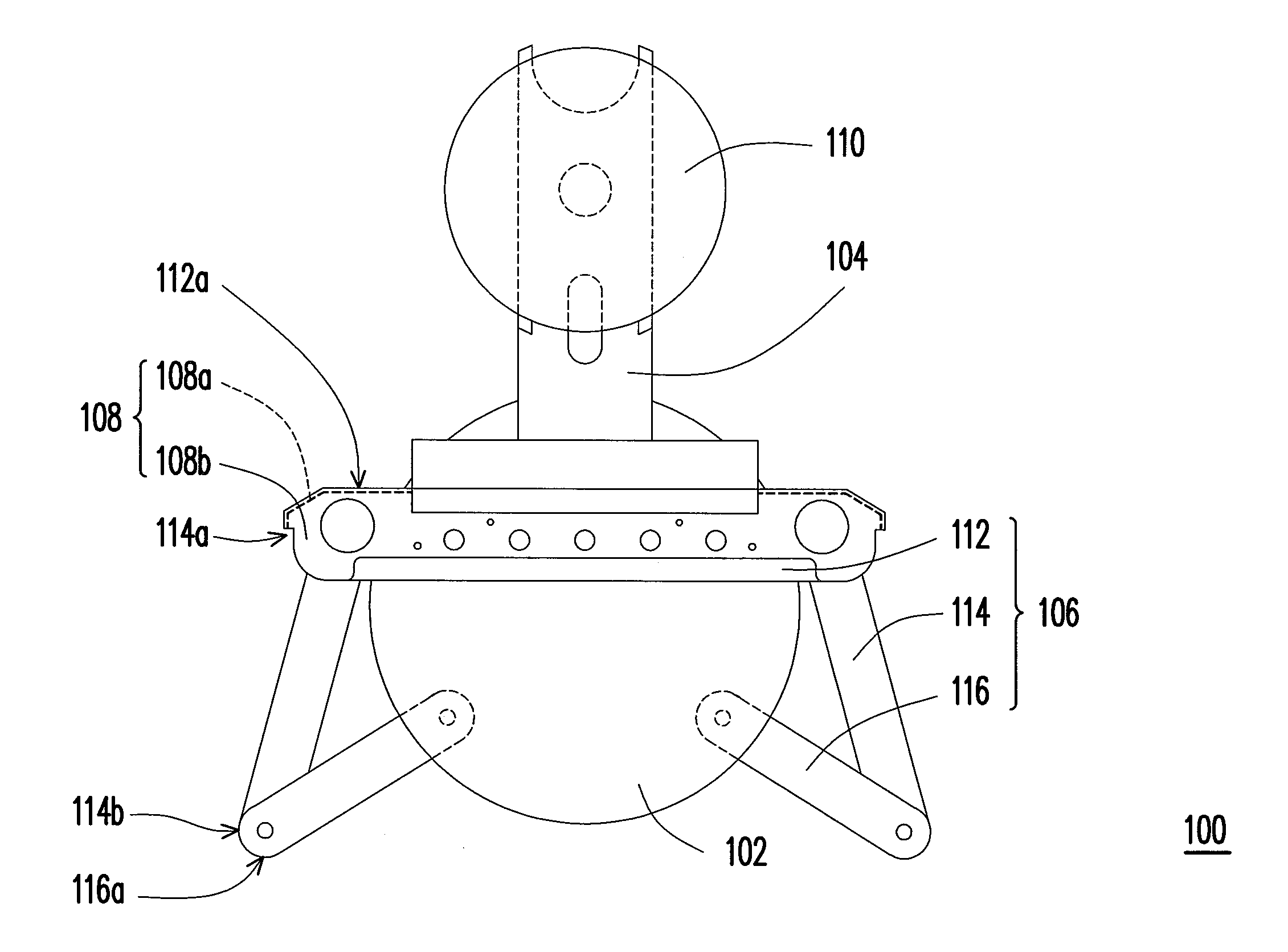
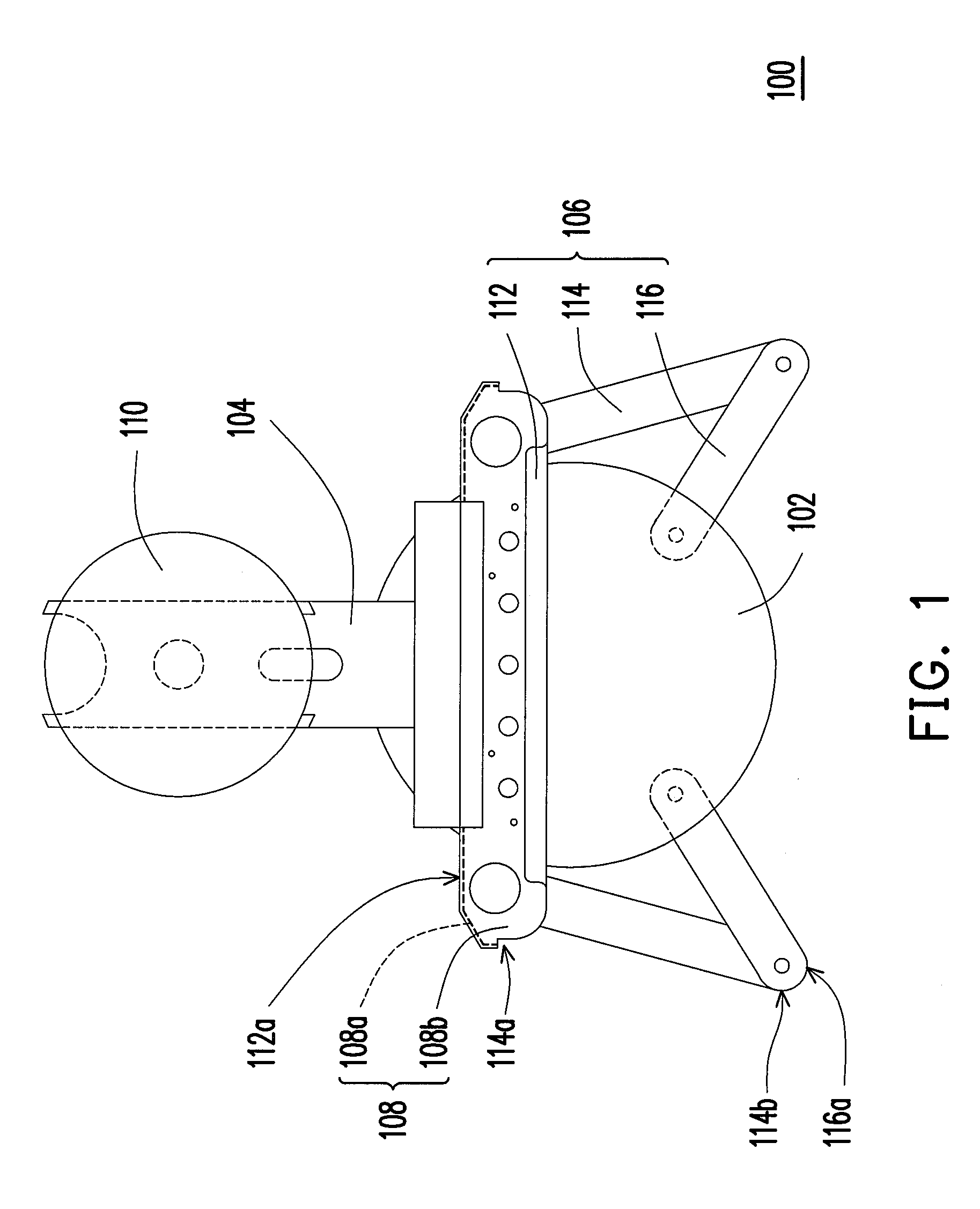
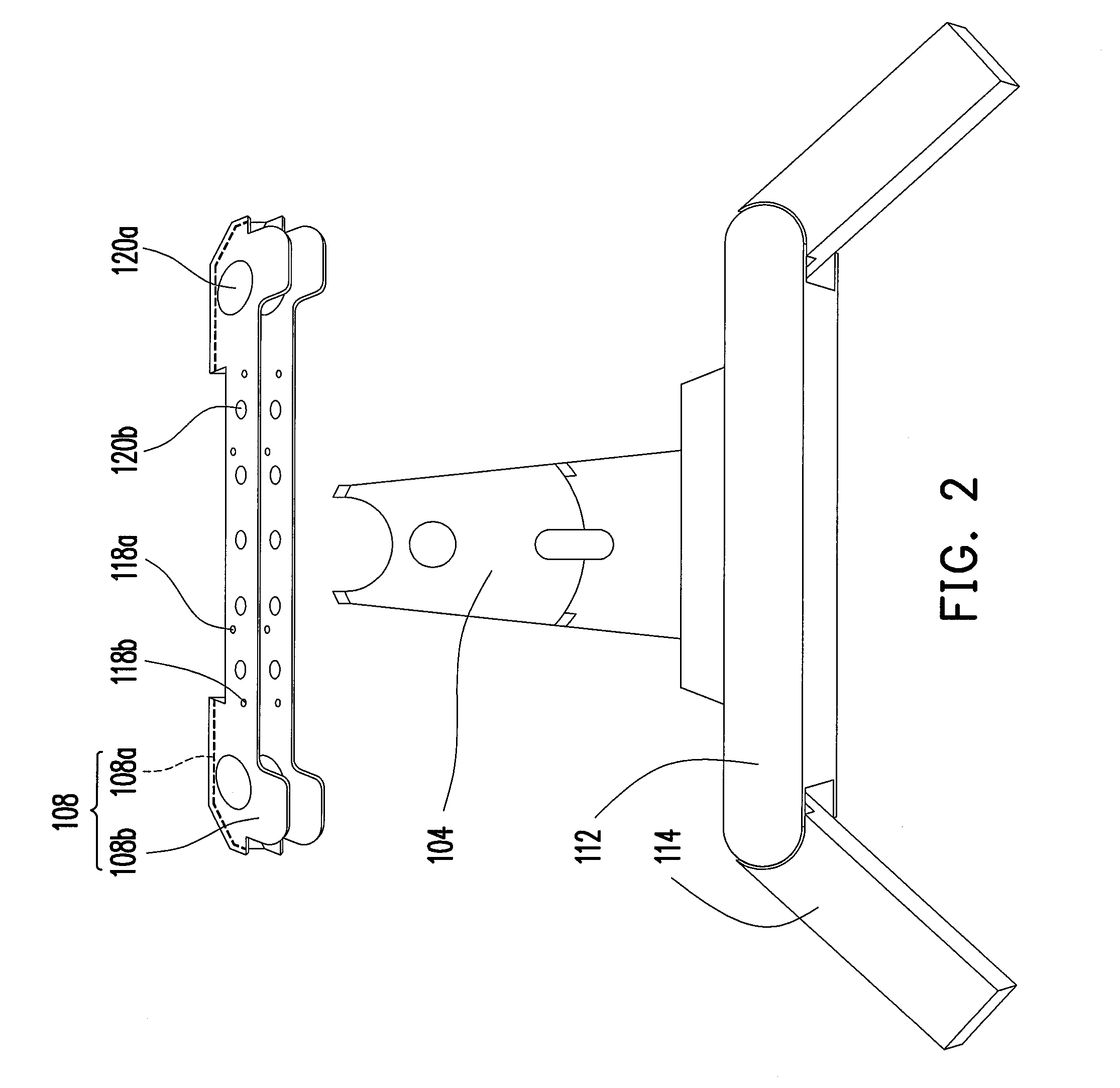
[0027]FIG. 1 is a schematic top view showing a wafer transfer apparatus according to one embodiment of the present invention. FIG. 2 is a schematic perspective view showing a portion of a wafer transfer apparatus according to one embodiment of the present invention. FIGS. 3A through 3C are schematic cross-sectional views showing a wafer transfer apparatus from different angles according to one embodiment of...
PUM
 Abstract
Description
Claims
Application Information