Transmission electron microscope apparatus comprising electron spectroscope, sample holder, sample stage, and method for acquiring spectral image

Inactive Publication Date: 2011-06-30
HITACHI HIGH-TECH CORP
View PDF4 Cites 8 Cited by
  • Summary
  • Abstract
  • Description
  • Claims
  • Application Information

AI Technical Summary

Benefits of technology

[0024]According to the present invention, a transmission electron microscope apparatus, a sample holder and a sample stage and a spectral image acquisition method as well which c

Problems solved by technology

With working dimensions of a silicon semiconductor, a magnetic device and the like reduced minutely and with high integration advanced, degradation in device characteristics and decrease in reliability have brought about more important problems than before.
In the case of the above method, however, the aberration of electron energy loss spectrum and the origin position will change owing to a drift of accelerating voltage of the electron beam concomitant with a change in external disturbance in the neighbor of the apparatus and with changes in magnetic field and electric field, making it difficult to compare the shape of energy loss near-edge structure of electron energy loss spectrum and a slight chemical shift as well at a measurement location with those at another measurement location.
In the aforementioned technique, the energy shift (drift) concomitant to the change of apparatus external disturbance or the like during the measurement is corrected and then the electron energy loss spectra are measured but a spectrum used for detection of the shift amount and a spectrum

Method used


Image

  • Transmission electron microscope apparatus comprising electron spectroscope, sample holder, sample stage, and method for acquiring spectral image
  • Transmission electron microscope apparatus comprising electron spectroscope, sample holder, sample stage, and method for acquiring spectral image
  • Transmission electron microscope apparatus comprising electron spectroscope, sample holder, sample stage, and method for acquiring spectral image

Examples


Embodiment Construction

[0034]Embodiments for carrying out the present invention will now be described with reference to the drawings. In all of the drawings for explaining the embodiments, identical parts are designated by identical reference numerals and their description will be omitted partly.

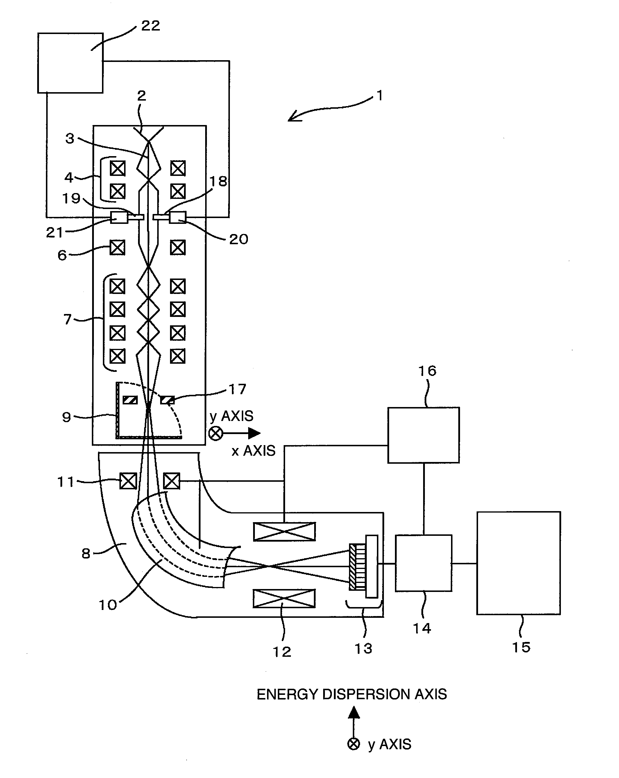
[0035]The schematic construction of a transmission electron microscope apparatus according to one embodiment of the present invention is illustrated diagrammatically in FIG. 1. The transmission electron microscope apparatus 1 has an electron spectrometer 8.

[0036]The transmission electron microscope apparatus 1 of the present embodiment comprises an electron gun having an electron source 2 and adapted to emit an electron beam 3, a condenser lens 4, an objective lens 6, an image-forming lens system 7 (image-forming lenses), a phosphor plate 9, the electron spectrometer 8, an image display unit 14, a data memory unit 15 and a central control unit 16. Between condenser lens 4 and objective lens 6, a plurality of sampl...


PUM


Abstract

A transmission electron microscope apparatus, a sample holder and a sample stage and a method for acquiring spectral images as well are provided which can acquire spectral images at a time from a plurality of samples and measure highly accurate chemical shifts from electron energy loss spectra extracted from the spectral images.
A transmission electron microscope apparatus comprises an electron gun for emitting an electron beam, a condenser lens for converging the emitted electron beam, a plurality of sample stages radiated with a converged electron beam and adapted to mount samples, a sample movement control unit for moving the sample stages, image-forming lenses for forming an image of an electron beam having transmitted through the plural samples, an electron spectrometer adapted to perform spectrometry of the electron beam in accordance with energy amounts the image-formed electron beam has and deliver spectral images obtained at convergence positions which are different in energy dispersion axis direction and in a direction orthogonal to the energy dispersion axis direction to thereby acquire spectral images from the plural samples at a time, and an image display unit for displaying acquired spectral images.

Description

TECHNICAL FIELD[0001]The present invention relates to a transmission electron microscope apparatus having an electron spectrometer, a sample holder and a sample stage and to a spectral image acquisition method as well which can acquire spectral images at a time from a plurality of samples and measure highly accurate chemical shifts from electron energy loss spectra extracted from the spectral images.BACKGROUND ART[0002]With working dimensions of a silicon semiconductor, a magnetic device and the like reduced minutely and with high integration advanced, degradation in device characteristics and decrease in reliability have brought about more important problems than before. In recent years, in order to analyze defects of semiconductor device in a nanometer region and ascertain causes of defects thoroughly to solve them in the course of development of new processes and mass-production, spectral analysis and two-dimensional element distribution analysis using (scanning) transmission ele...

Claims


Application Information

Patent Timeline
IPC IPC(8): H01J37/26H01J37/20
CPCH01J37/20H01J37/244H01J37/28H01J2237/2802H01J2237/20264H01J2237/2446H01J2237/24485H01J2237/201
Inventor TERADA, SHOHEITANIGUCHI, YOSHIFUMAI
Owner HITACHI HIGH-TECH CORP
Why Eureka
Try Eureka