Semiconductor Devices Comprising a Plurality of Gate Structures

a gate structure and semiconductor technology, applied in the direction of semiconductor devices, transistors, electrical devices, etc., can solve the problems of reducing the speed of memory devices, degrading the reliability of memory devices, and increasing parasitic capacitance between adjacent structures in memory cell regions, so as to reduce/minimize parasitic capacitance and variance, the volume of gaps may be increased/maximized, and the effect of reducing the varian

Active Publication Date: 2011-07-07
SAMSUNG ELECTRONICS CO LTD
View PDF10 Cites 22 Cited by
  • Summary
  • Abstract
  • Description
  • Claims
  • Application Information

AI Technical Summary

Benefits of technology

As a result of the embodiments, the volume of the gaps may be increased / maximized in order to reduce / minimize the parasitic capacitance and any variance therein between the gate structures.

Problems solved by technology

Unfortunately, these efforts often result in increased parasitic capacitance between adjacent structures in the memory cell regions.
Such increases in parasitic capacitance reduce the speed of the memory devices.
Also, variation in parasitic capacitance between gate structures causes a variation in the threshold voltage for each gate structure, thereby degrading the reliability of memory devices.
One disadvantage of these approaches is that the area between adjacent gates is largely filled with an oxide dielectric layer with a relatively small air pocket.

Method used


Image

  • Semiconductor Devices Comprising a Plurality of Gate Structures
  • Semiconductor Devices Comprising a Plurality of Gate Structures
  • Semiconductor Devices Comprising a Plurality of Gate Structures

Examples


Embodiment Construction

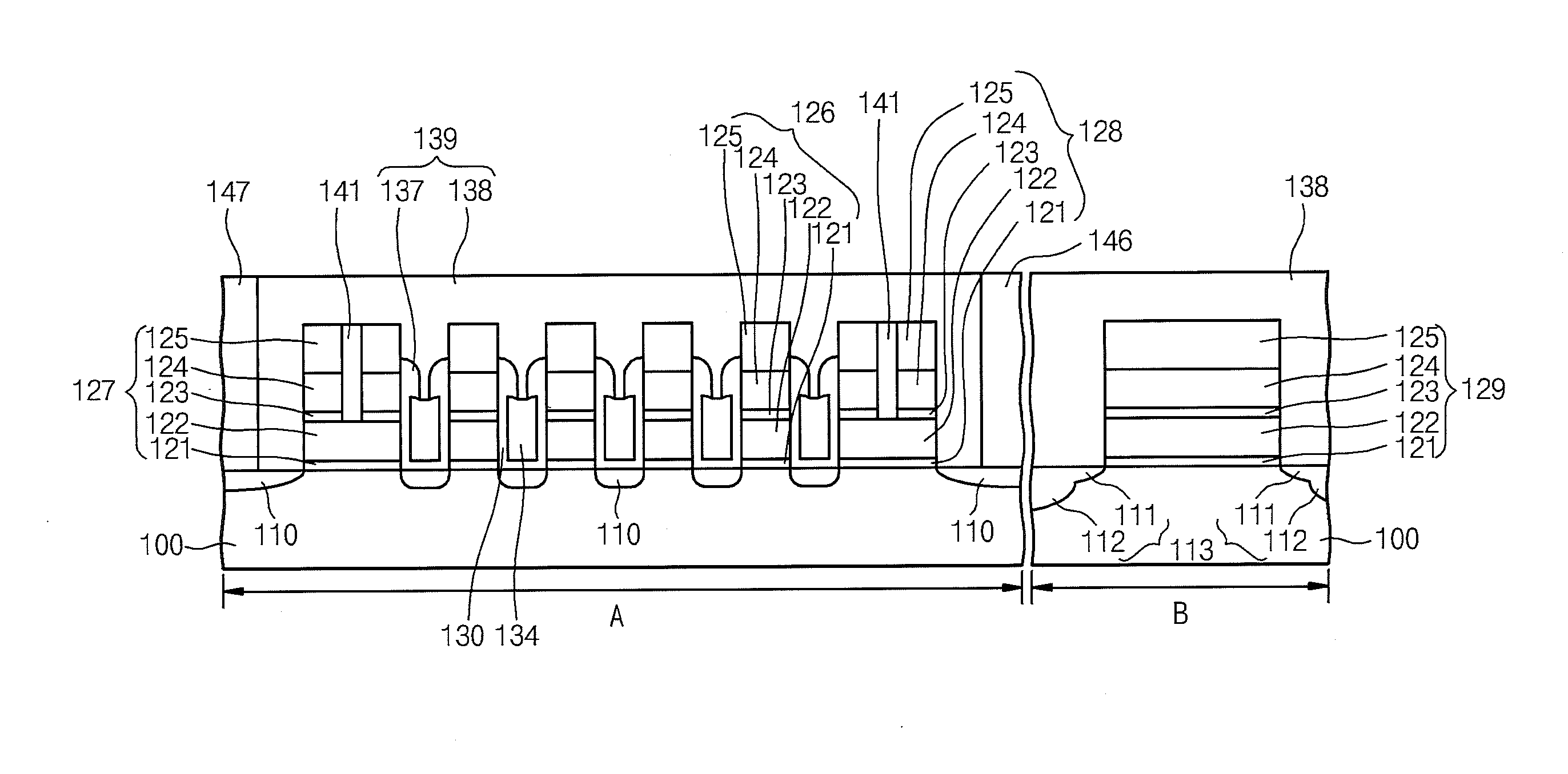
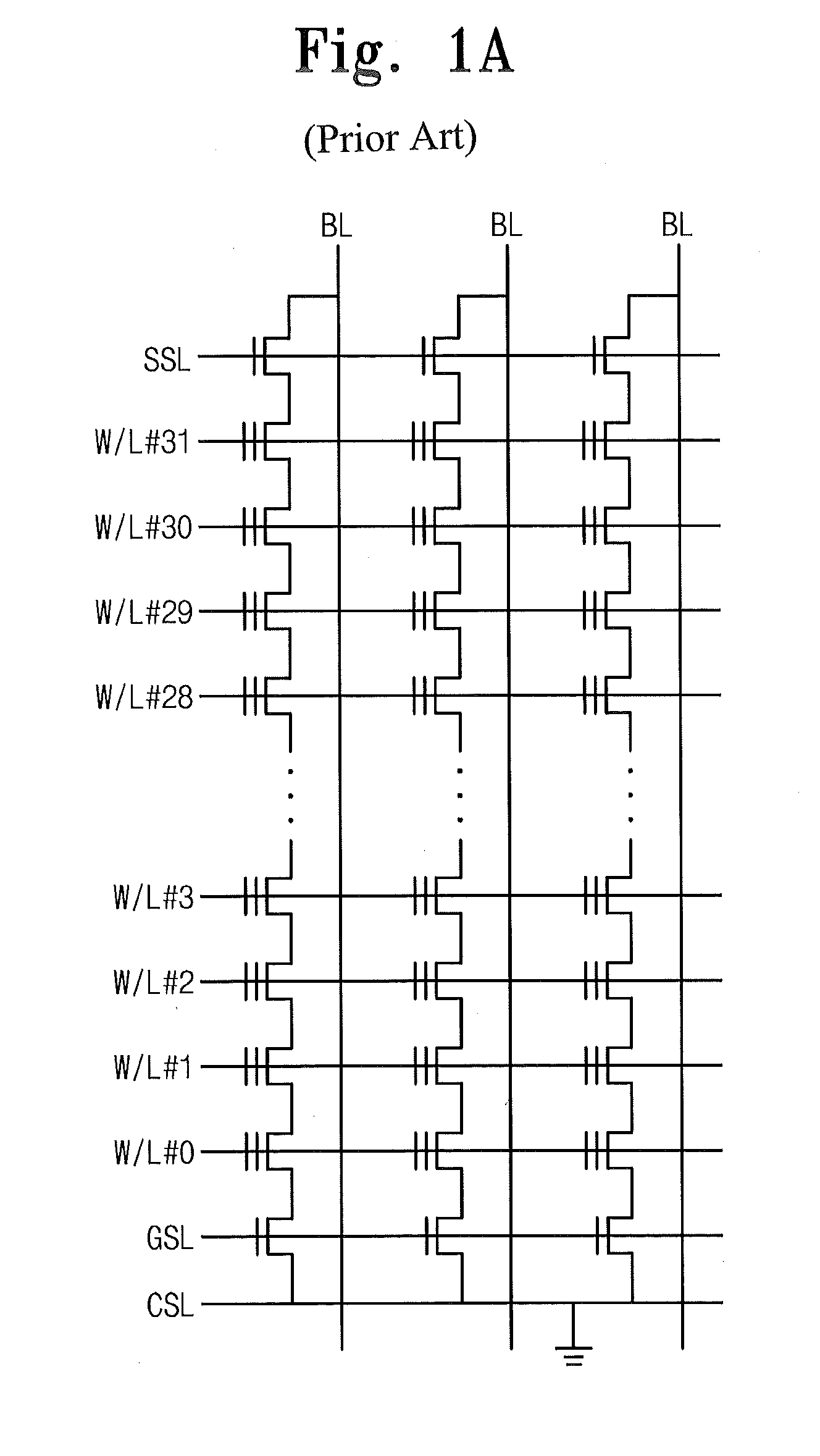
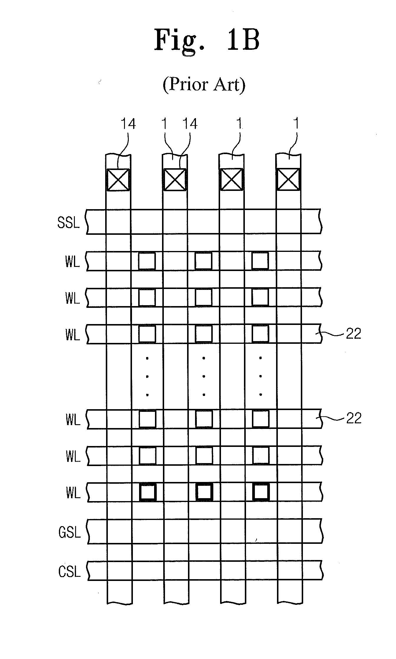
Example embodiments are described below with reference to the accompanying drawings. Many different forms and embodiments are possible without deviating from the spirit and teachings of this disclosure and so the disclosure should not be construed as limited to the example embodiments set forth herein. Rather, these example embodiments are provided so that this disclosure will be thorough and complete, and will convey the scope of the disclosure to those skilled in the art. In the drawings, the sizes and relative sizes of layers and regions may be exaggerated for clarity. Like reference numbers refer to like elements throughout.

Example embodiments are described herein with reference to cross-section illustrations that are schematic illustrations of idealized example embodiments (and intermediate structures). As such, variations from the shapes of the illustrations as a result, for example, of manufacturing techniques and / or tolerances, are to be expected. Thus, example embodiments m...


PUM


Abstract

Semiconductor devices are provided. The semiconductor devices may include a plurality of gate structures disposed on a semiconductor substrate, each of the gate structures including a floating gate, an inter-gate dielectric layer, and a control gate. The semiconductor devices may also include liners on opposing sidewalls of adjacent ones of the gate structures. The liners may define a gap. A first width of the gap may be less than a second width of the gap.

Description

BACKGROUND1. Technical FieldThis disclosure generally relates to semiconductor devices and, more particularly, to semiconductor memory devices and methods of fabricating the same.2. Description of the Related ArtAmong semiconductor devices, non-volatile memory devices are commonly used in consumer electronic devices because information can be retained in the device even when no power is supplied. Advances in consumer electronics cause demand for ever higher density memory devices. Efforts to manufacture devices meeting this demand often involve scaling down the sizes of gate structures and reducing the space between adjacent gate structures.Unfortunately, these efforts often result in increased parasitic capacitance between adjacent structures in the memory cell regions. Such increases in parasitic capacitance reduce the speed of the memory devices. Also, variation in parasitic capacitance between gate structures causes a variation in the threshold voltage for each gate structure, t...

Claims


Application Information

Patent Timeline
Patent Type & Authority Applications(United States)
IPC IPC(8): H01L29/788
CPCH01L21/764H01L21/823456H01L21/823468H01L27/115H01L27/11573H01L27/11524H01L27/11526H01L27/11529H01L27/11568H01L27/11521H10B41/40H10B41/41H10B69/00H10B41/30H10B41/35H10B43/40H10B43/30
Inventor KANG, DAE-WOONGCHANG, SUNG-NAMKIM, JIN-JOOLEE, KYONG-JOOLEE, EUN-JUNG
Owner SAMSUNG ELECTRONICS CO LTD
Why Eureka
Try Eureka