Passive component

Active Publication Date: 2011-07-07
SOSHIN ELECTRIC
View PDF12 Cites 1 Cited by
  • Summary
  • Abstract
  • Description
  • Claims
  • Application Information

AI Technical Summary

Benefits of technology

As described above, the passive component according to the present invention may be designed in various modes. For example, even if each of the unbalanced line and the balanced line has an electrical length λ/2, the physical length of the balanced line can be made smaller than the physical length of the unbalanced line. Alternatively, even if the unbalanced line and the balanced line have different electrical lengths, the physical lengths of the unbalanced line and the balanced line can be made equal to each other. Therefore, the unbalanced to balanced converter can be designed with an increased degree of freedom.
With the passive component according to the present invention, furthermore, one resonance electrode can also function as the

Problems solved by technology

However, the stacked bandpass filter disclosed in Japanese Laid-Open Patent Publication No. 2005-080248 is problematic in that it suffers a low degree of design freedom.
Therefore, the degree of design freedom is limited.
Accordingly, the disclosed stacked bandpass filter may not be able to meet various requirements.
Even if the disclosed stacked bandpass filter can meet various requirements, it suffers problems in that it causes a large loss and has a

Method used


Image

  • Passive component
  • Passive component
  • Passive component

Examples


Example

Embodiment 1

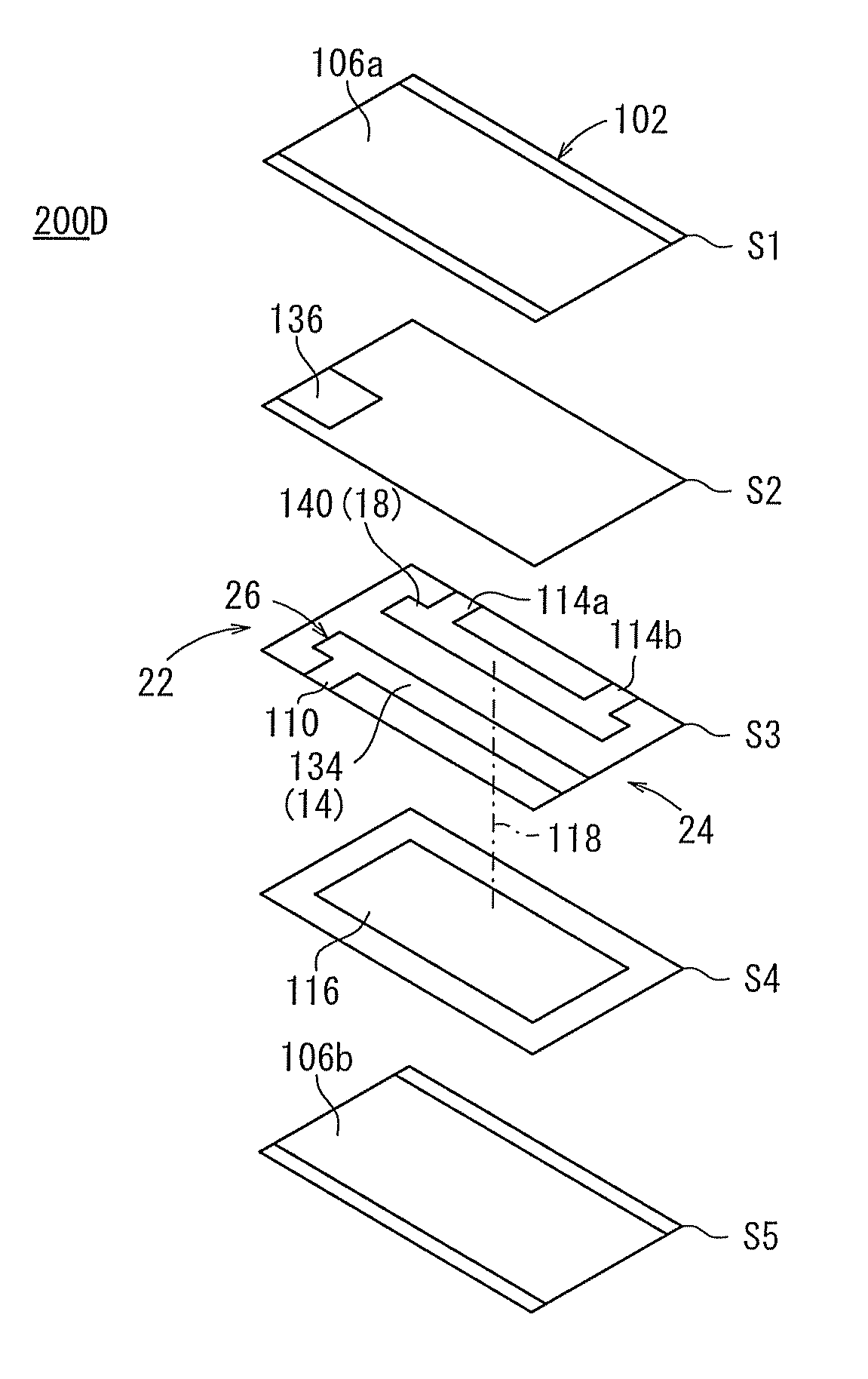
A balun according to Embodiment 1 (hereinafter referred to as “first balun 100A”) represents a first specific example of the second passive component 10B. As shown in FIG. 9, the first balun 100A has a dielectric substrate 102 comprising a plurality of dielectric layers stacked and sintered together. The dielectric substrate 102 has outer surfaces including a first side surface 102a with an unbalanced input terminal 12 disposed thereon, a second side surface 102b (a side surface facing the first side surface 102a) with two balanced output terminals (a first balanced output terminal 16a and a second balanced output terminal 16b) disposed thereon, and a third side surface 102c and a fourth side surface 102d with shield terminals 104 disposed respectively thereon.

As shown in FIG. 10, the dielectric substrate 102 comprises first through fifth dielectric layers S1 through S5 which are stacked successively from above. Each of the first through fifth dielectric layers S1-S5 com...

Example

Embodiment 2

A balun according to Embodiment 2 (hereinafter referred to as “second balun 100B”) represents a second specific example of the second passive component 10B. The second balun 100B is of substantially the same structure as the first balun 100A, but is different therefrom as follows:

As shown in FIG. 11, the second balun 100B includes an unbalanced input terminal 12 and a DC voltage input terminal (DC input terminal 120) which are disposed on the first side surface 102a among the outer surfaces of the dielectric substrate 102.

As shown in FIG. 12, the capacitor-forming electrode 116 is connected to the DC input terminal 120 through a lead electrode 122, and also functions as an electrode (DC electrode 124) to which a DC voltage is applied. Therefore, the first balanced output terminal 16a and the second balanced output terminal 16b output balanced output signals including the DC voltage applied to the DC electrode 124 as a bias voltage.

Example

Embodiment 3

A balun according to Embodiment 3 (hereinafter referred to as “third balun 100C”) represents a third specific example of the second passive component. The third balun 100C is of substantially the same structure as the first balun 100A, but is different therefrom as follows:

As shown in FIG. 13, the dielectric substrate 102 comprises first through sixth dielectric layers S1 through S6 which are stacked successively from above.

The second stripline electrode 112 is disposed on the principal surface of the third dielectric layer S3. A first matching circuit element 126A and a second matching circuit element 126B for matching the output impedance with the input impedance of an external circuit are disposed on the principal surface of the fourth dielectric layer S4.

The first matching circuit element 126A includes a first inductance electrode 128a having a spiral shape and a first lead electrode 114a which connects the first inductance electrode 128a to the first balanced output...


PUM


Abstract

A first passive component includes one unbalanced line having one unbalance input terminal, one balanced line installed opposite to the unbalanced line and having two balanced output terminals (first balanced output terminal and second balanced output terminal, and a capacitor formed between the balanced line and a fixed potential (e.g. the ground potential). Furthermore, the relation d1>d2 is satisfied, where d1 is the physical length of the unbalanced line and d2 is the physical length of the balanced line.

Description

TECHNICAL FIELDThe present invention relates to a passive component, and more particularly to a passive component suitable for use in an unbalanced to balanced converting circuit for converting an unbalanced output signal into a balanced output signal or for use in a composite circuit which includes a filter having at least one resonator and an unbalanced to balanced converting circuit.BACKGROUND ARTGenerally, there is known a balun transformer (unbalanced to balanced converter) as a circuit component for converting an unbalanced input signal into a balanced output signal or converting a balanced input signal into an unbalanced output signal.Recently, semiconductor components such as integrated circuits (ICs) or the like have been highly integrated, while semiconductor components have quickly become smaller in their size. Accordingly, balun transformers have also become smaller in size.One conventional balun transformer has a ½-wavelength unbalanced transmission line and a pair of ¼...

Claims


Application Information

Patent Timeline
IPC IPC(8): H03H5/00
CPCH01P5/10H01P1/203H01P1/205
Inventor URANO, MASAKITAKEUCHI, HIROTAKA
Owner SOSHIN ELECTRIC
Why Eureka
Try Eureka