Method of production of circuit board utilizing electroplating

Active Publication Date: 2006-10-05
SHINKO ELECTRIC IND CO LTD
View PDF11 Cites 10 Cited by
  • Summary
  • Abstract
  • Description
  • Claims
  • Application Information

AI Technical Summary

Benefits of technology

[0030] According to the method of production of a circuit board utilizing electroplating of the present invention, unlike a circuit board produced by the conventional method of production, plating interconnects are no longer required. In addition, there are no “unnecessary parts” such as connection parts for connecting the circuit patterns to the plating interconne

Problems solved by technology

As stated above, with a circuit board produced by the above conventional subtractive method, unnecessary parts are formed in the circuit patterns due to the need to feed power for electroplating.
These unnecessary pa

Method used


Image

  • Method of production of circuit board utilizing electroplating
  • Method of production of circuit board utilizing electroplating
  • Method of production of circuit board utilizing electroplating

Examples


Example

First Embodiment

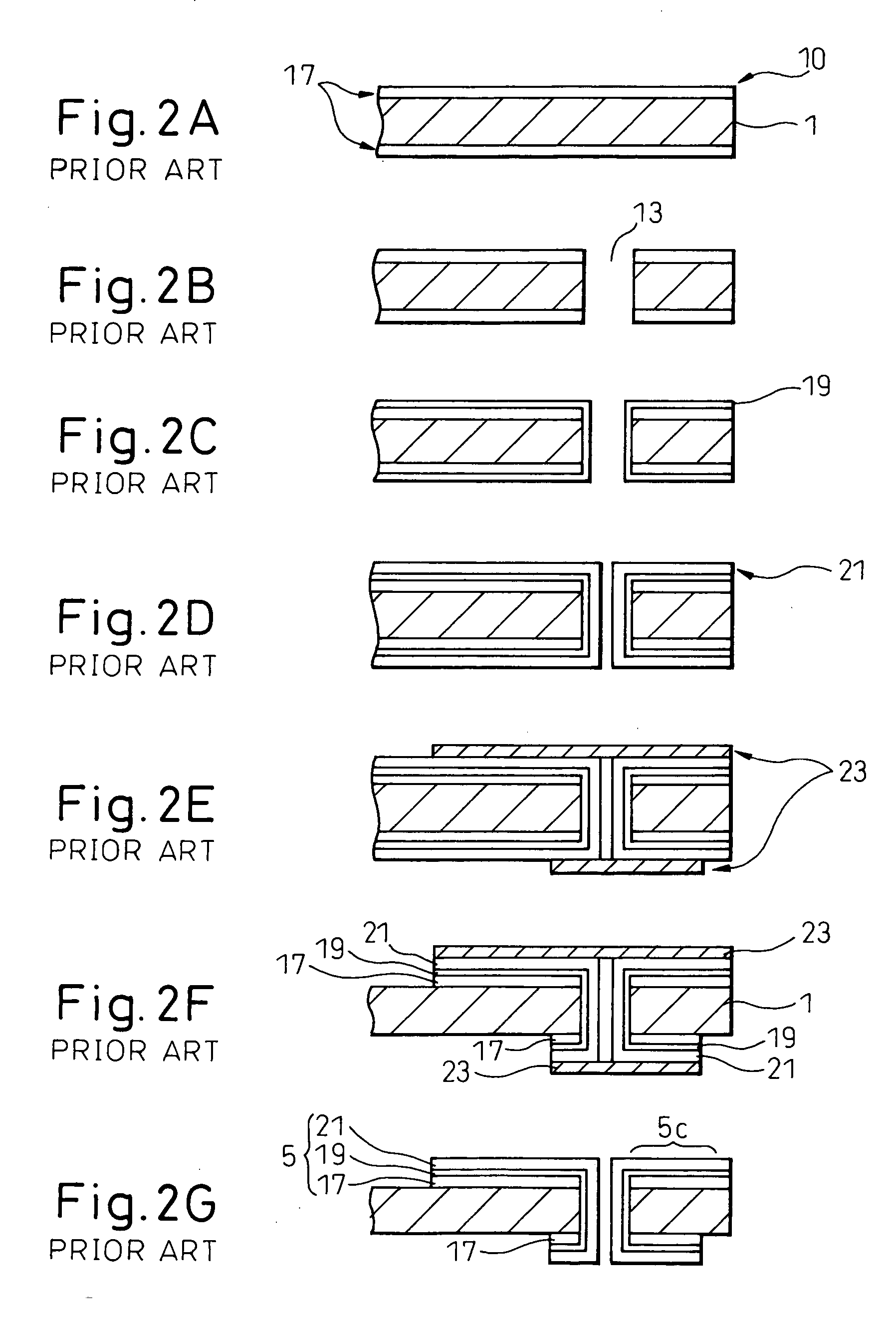
[0040] Below, a first embodiment of the present invention will be explained with reference to FIGS. 4A to 4N. In the following explanation, the dimensions of the different parts are only representative examples. There is no need to limit the invention to these dimensions.

[0041] First, as shown in FIG. 4A, a double-sided copper foil 17 (thickness 1 to 31 μm)—clad glass cloth—containing epoxy resin board 1 (thickness 0.03 mm or more) is prepared.

[0042] Next, as shown in FIG. 4B, a drill is used to form through holes 13 (opening diameter 35 to 350 μm) in the board 1.

[0043] Next, as shown in FIG. 4C, a first copper electroless plating layer 51 (thickness 0.01 μm or more) is formed on the copper foil 17 and in the through holes 13. The first copper electroless plating layer 51 later forms the power feed layer for the copper electroplating. 0.01 μm or so of thickness is sufficient for functioning as a power feed layer. The first copper electroless plating layer 51 may ...

Example

Second Embodiment

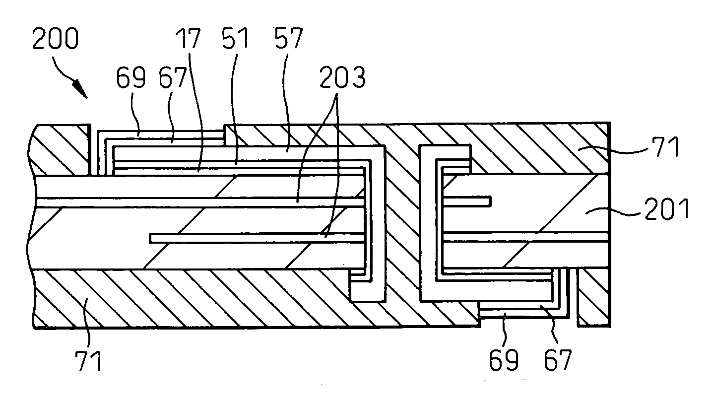
[0065] The method of the present invention may also use a double-sided copper foil-clad multilayer board.

[0066] First, as shown in FIG. 6A, a double-sided copper foil-clad multilayer board 201 (thickness 80 to 500 μm or so) comprised of a glass cloth-containing epoxy resin board on the two surfaces of which copper foil 17 (thickness 1 to 3 μm) is clad and formed inside with circuit patterns 203 is prepared.

[0067] Next, as shown in FIG. 6B, this board 201, in the same way as the first embodiment, is formed with through holes 13 (opening diameter 35 to 350 μm or so).

[0068] Next, as shown in FIG. 6C, in the same way as the first embodiment, the first copper electroless plating layer 51 (thickness 0.01 μm or more) is formed.

[0069] After this, processing is performed in the same way as the steps of the first embodiment shown in FIG. 4D to FIG. 4N, whereby the multilayer circuit board 200 shown in FIG. 6D is completed. This structure is similar to the structure of th...


PUM


Abstract

A method of production of a circuit board utilizing electroplating which prevents signal reflection and noise due to unnecessary parts in the circuit patterns when electroplating to form circuit patterns on the board to thereby improve the electrical properties and realize higher density layout of the circuit patterns, including the steps of forming a first electroless plating layer and an overlying first plating resist on a metal foil-clad insulating board, feeding power to the first electroless plating layer to form a first electroplating layer over the first electroless plating layer in resist openings; removing the first plating resist; removing the exposed first electroless plating layer and metal foil to expose the insulating board; forming a second electroless plating layer over the exposed parts of the board and the circuit patterns; forming a second plating resist over that; removing the second electroless plating layer at the resist openings; feeding power to the second electroless plating layer under the second plating resist to form a second electroplating layer over the circuit patterns in the resist openings; removing the second plating resist; and removing the exposed second electroless plating layer.

Description

BACKGROUND OF THE INVENTION [0001] 1. Field of the Invention [0002] The present invention relates to a method of production of a circuit board used for a semiconductor device etc., more particularly relates to a method of production of a circuit board not requiring power feed plating interconnects when producing a circuit board utilizing electroplating. [0003] 2. Description of the Related Art [0004] In the past, when producing circuit boards used for semiconductor devices, for example, a large board 1 comprised of a glass prepreg or other resin as shown in FIG. 1A was prepared, this large board 1 was formed with circuit patterns 5 corresponding to a plurality of circuit boards 3 in a matrix, then this was cut along predetermined cutting lines 7 so as to obtain the individual circuit boards 3. [0005] In particular, when using the subtractive method (tenting method) to form circuit patterns on the large board 1, since the bonding pads and other main parts of the circuit patterns 5 ar...

Claims


Application Information

Patent Timeline
IPC IPC(8): C25D5/18
CPCH05K3/108H05K3/243H05K3/427H05K2203/0542H05K2203/0723Y10T29/49165H01L2224/48091H01L2224/48227H01L2924/15311H05K2203/1394H01L2924/00014F21V3/02F21V15/01F21V17/101F21V17/12
Inventor OKAZAWA, HIDEYASUTAKEDA, YOSHIKI
Owner SHINKO ELECTRIC IND CO LTD
Why Eureka
Try Eureka