Demodulation Sensor with Separate Pixel and Storage Arrays

a technology of demodulation sensor and storage array, which is applied in the field of demodulation sensor with separate pixel and storage array, can solve the problems of pixel pitch of 10 micrometers or less becoming almost impossible without compromise in distance resolution and accuracy, and pixel pitch of 10 micrometers or less becoming almost impossible without significant reduction of pixel fill factor, so as to reduce storage nodes even smaller, reduce pixel size, and reduce the effect of pixel siz

Active Publication Date: 2011-07-07
AMS SENSORS SINGAPORE PTE LTD
View PDF23 Cites 48 Cited by
  • Summary
  • Abstract
  • Description
  • Claims
  • Application Information

AI Technical Summary

Benefits of technology

[0011]The presented invention solves the problem of shrinking the pixel size without significantly reducing the pixel's fill factor and without compromising the image quality by making the storage nodes even smaller. The solutio...

Problems solved by technology

A common problem for all demodulation pixels used in demodulation sensors, such as for TOF imaging or FLIM, or otherwise, arises when trying to shrink the pixel size to realize arrays of higher pixel counts.
Since the storage nodes require a certain area in the pixel in order to maintain adequate storage capacity and thus image quality, the pixel's fill factor suffers from the shrinking process associated with moving to these larger array...

Method used


Image

  • Demodulation Sensor with Separate Pixel and Storage Arrays
  • Demodulation Sensor with Separate Pixel and Storage Arrays
  • Demodulation Sensor with Separate Pixel and Storage Arrays

Examples


Embodiment Construction

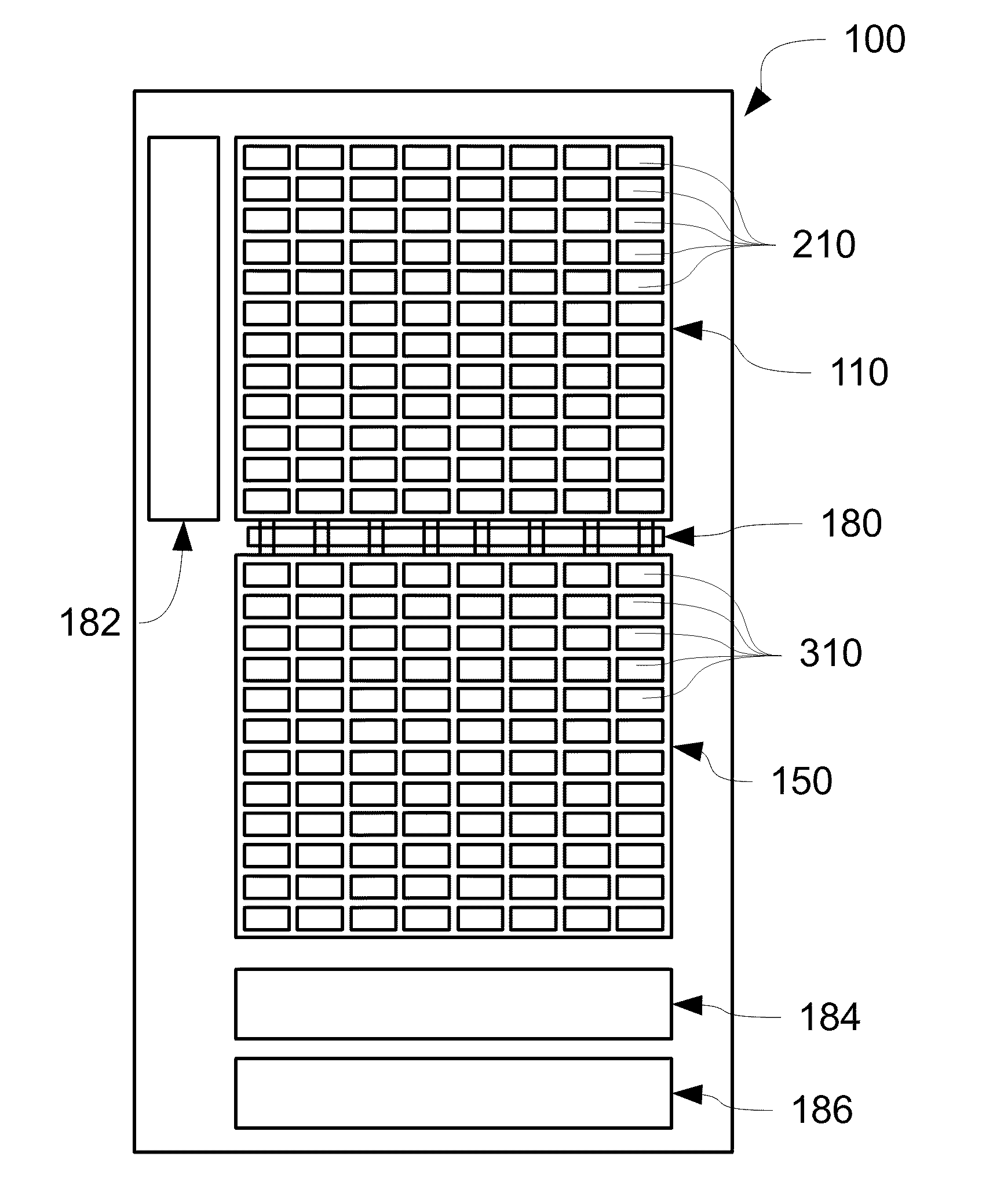
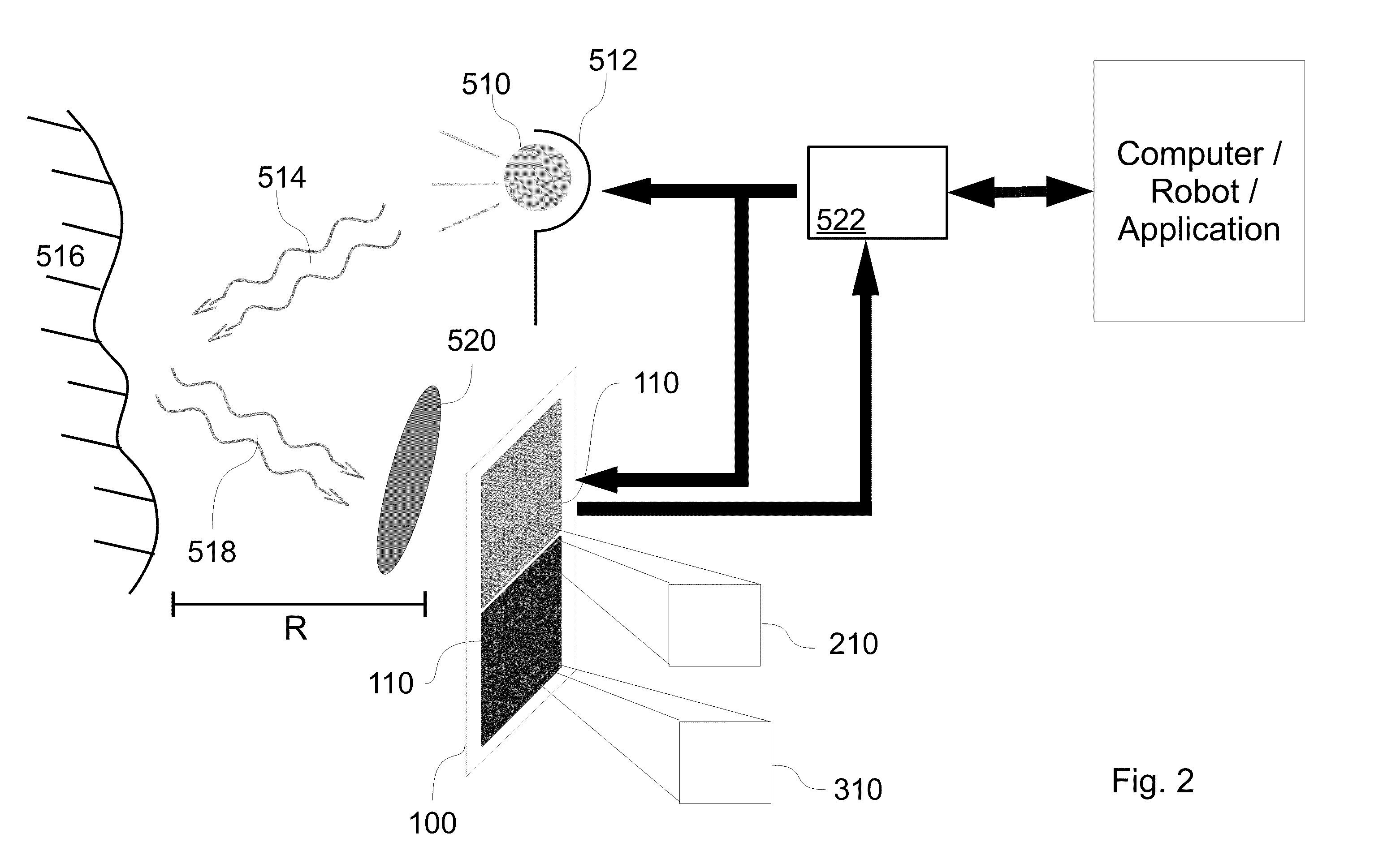
[0037]FIG. 1 shows a demodulation sensor 100 that has been constructed according to the principles of the present invention.

[0038]The illustrated architecture extracts elements, which are typically integrated inside the pixel but not necessarily required for the photo detection, out of the pixel into physically separated elements that are basically storage and sometimes processing elements, termed storage elements or proxels. As a consequence, the sensor includes a pixel array 110 of x×y pixels and a storage or proxel array 150 of x×y of storage elements or proxels 310 that are used for further processing, storage of the information and readout. Usually x and y are greater than 100, and preferably greater than 200. In some examples x, y are greater than 1000. The two arrays are physically separated from each other in preferably discrete arrays that do not physically overlap with each other on the chip.

[0039]Multiple functions are preferably handled in this proxel array 150. Thus, th...


PUM


Abstract

A demodulation image sensor, such as used in time of flight (TOF) cameras, extracts all storage- and post-processing-related steps from the pixels to another array of storage and processing elements (proxels) on the chip. The pixel array has the task of photo-detection, first processing and intermediate storage, while the array of storage and processing elements provides further processing and enhanced storage capabilities for each pixel individually. The architecture can be used to address problems due to the down-scaling of the pixel size. Typically, either the photo-sensitivity or the signal storage capacitance suffers significantly. Both a lower sensitivity and smaller storage capacitances have negative influence on the image quality. The disclosed architecture allows for keeping the storage capacitance unaffected by the pixel down-scaling. In addition to that, it provides a high degree of flexibility in integrating more intelligence into the image sensor design already on the level of the pixel array. In particular, if applied to demodulation pixels, the flexibility of the architecture allows for integrating on sensor-level concepts for multi-tap sampling, mismatch compensation, background suppression and so on, without any requirement to adjust the particular demodulation pixel architecture.

Description

RELATED APPLICATIONS[0001]This application claims the benefit under 35 USC 119(e) of U.S. Provisional Application No. 61 / 292,588, filed on Jan. 6, 2010, which is incorporated herein by reference in its entirety.BACKGROUND OF THE INVENTION[0002]Electronic imaging sensors usually have an array of m×n photo-sensitive pixels, with x>=1 rows and y>=1 columns. Each pixel of the array can individually be addressed by dedicated readout circuitry for column-wise and row-wise selection. Optionally a block for signal post-processing is integrated on the sensor.[0003]The pixels typically have four basic functions: photo detection, signal processing, information storage, and analog or digital conversion. Each of these functions consumes a certain area on the chip.[0004]A special group of smart pixels, called demodulation pixels, is well-known for the purpose of three dimensional (3D) imaging. Other applications of such demodulation pixels include fluorescence life-time imaging (FLIM). The ...

Claims


Application Information

Patent Timeline
IPC IPC(8): H04N7/18H01L27/146G01S7/4914G01S17/894
CPCG01S17/36G01S7/4914G01S7/4918G01S17/89G01S17/894
Inventor BUETTGEN, BERNHARDOGGIER, THIERRY
Owner AMS SENSORS SINGAPORE PTE LTD
Why Eureka
Try Eureka