Semiconductor light-emitting device

a technology of semiconductors and light-emitting devices, which is applied in the direction of semiconductor devices, basic electric elements, electrical appliances, etc., can solve the problems of high product deficiency or defect rate, and achieve the effects of stable operation, reduced reverse withstand voltage vr defect rate, and high yield

Active Publication Date: 2011-07-21
STANLEY ELECTRIC CO LTD
View PDF3 Cites 7 Cited by
  • Summary
  • Abstract
  • Description
  • Claims
  • Application Information

AI Technical Summary

Benefits of technology

[0007]Problems with AlGaInP-based LEDs include wide range of variation in the reverse withstand voltage Vr in the wafer surface, and thus a high product deficiency or defect rate, due to the tilt (“off-angle”) of the crystal plane relative to the predetermined crystal axis of the growth substrate and due to the semiconductor film growth conditions. The present inventors discovered that the disparities or variations in reverse withstand voltage Vr seen in AlGaInP-based LEDs are caused by the natural superlattice formed in the n-type clad layer. In other words, it was assumed that the ordered arrangement of Al atoms formed in the n-type clad layer exerts an influence on the reverse withstand voltage Vr. The inventors, believing the natural superlattice had to be suppressed in order to suppress the variations in the reverse withstand voltage Vr, and also taking into account light output, studied layered structures for the n-type clad layer.
[0008]An object of the present invention is to provide an AlGaInP-based semiconductor light-emitting device able to maintain light output, suppress variations in reverse withstand voltage Vr inside the wafer surface, and ensure high production yields.
[0010]The semiconductor light-emitting device according to the present invention is able to reduce the reverse withstand voltage Vr defect rate caused by the natural superlattice and to ensure a stable, high yield, despite the off-angle of the crystal plane of the growth substrate and the despite the growth conditions in an AlGaInP-based semiconductor light-emitting device and without compromising light output.

Problems solved by technology

Problems with AlGaInP-based LEDs include wide range of variation in the reverse withstand voltage Vr in the wafer surface, and thus a high product deficiency or defect rate, due to the tilt (“off-angle”) of the crystal plane relative to the predetermined crystal axis of the growth substrate and due to the semiconductor film growth conditions.

Method used


Image

  • Semiconductor light-emitting device
  • Semiconductor light-emitting device
  • Semiconductor light-emitting device

Examples


embodiments

[0028]There follows a description of embodiments of the present invention made with reference to the accompanying drawings. In the drawings indicated below, configurational elements and portions substantially identical or equivalent are denoted by the same reference numerals.

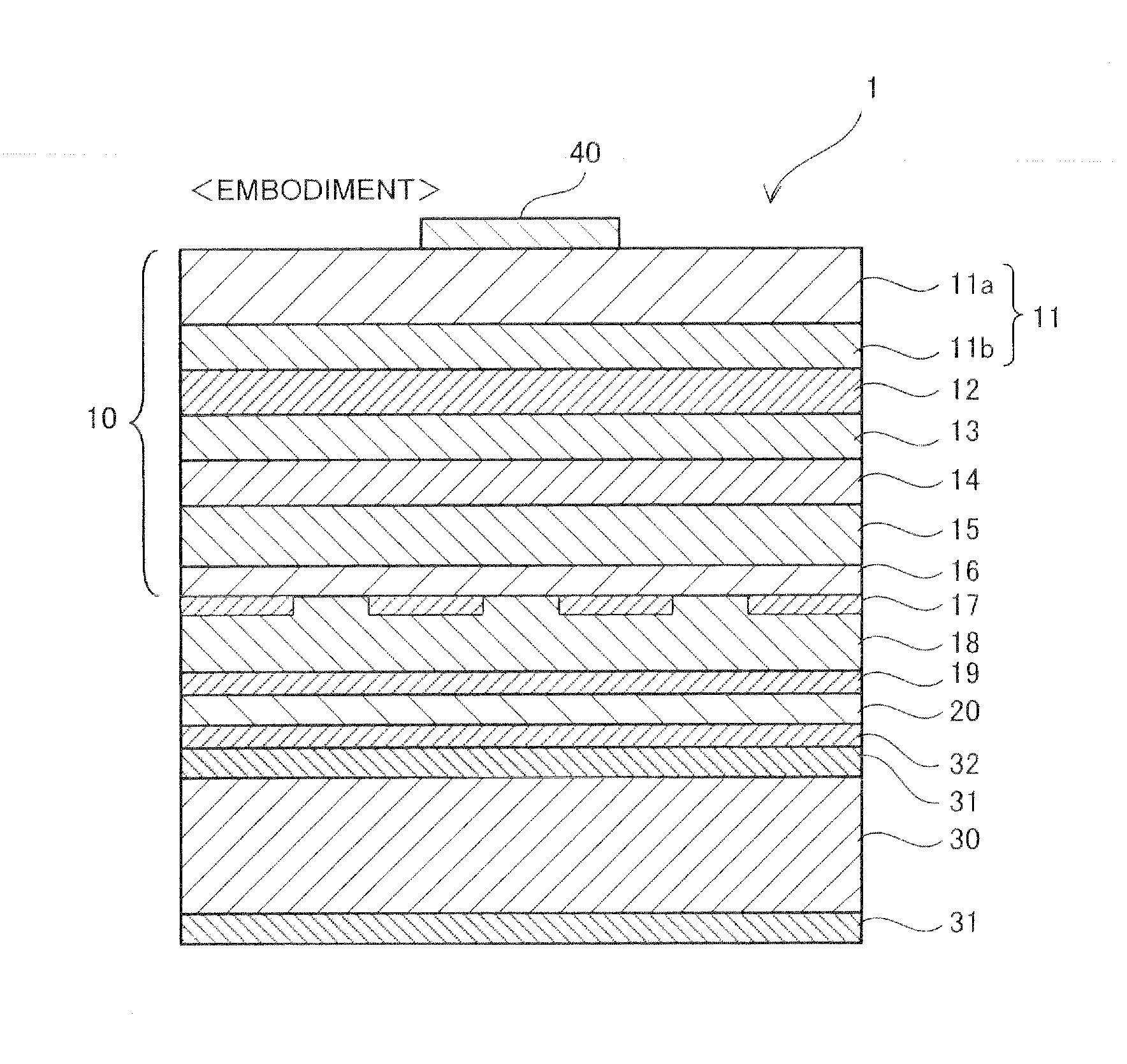
[0029]FIG. 1 is a cross-sectional view showing the configuration of a semiconductor light-emitting device 1 according to an embodiment of the invention. The light-emitting device 1 has a “joined” or “bonded” structure in which a semiconductor film 10 composed of an AlGaInP-based material is “joined” or “bonded” via a reflective electrode layer 18 to a conductive support substrate 30 which is prepared separately from a growth substrate used for crystal growth.

[0030]The semiconductor film 10 comprises an n-type clad layer 11 composed of a first n-type clad layer 11a and a second n-type clad layer 11b, an active layer 12, and a p-type clad layer 13. The active layer 12 is provided between the second n-type clad lay...


PUM


Abstract

The device including an active layer composed of AlGaInP, and an n-type clad layer and a p-type clad layer disposed so as to sandwich the active layer, the n-type clad layer and the p-type clad layer each having a bandgap greater than the bandgap of the active layer. The n-type clad layer includes a first n-type clad layer composed of AlGaInP and a second n-type clad layer composed of AlInP; and the second n-type clad layer has a thickness in the range from 40 nm to 200 nm.

Description

BACKGROUND OF THE INVENTION[0001]1. Technical Field[0002]The present invention relates to a semiconductor light-emitting device such as a light-emitting diode (LED), and more particularly to a semiconductor light-emitting device having an AlGaInP-based semiconductor film.[0003]2. Description of the Related Art[0004]Improvements in light-emitting efficiency have expanded the applications for AlGaInP-based LEDs as light sources for display and lighting such as rear combination lamps for automobiles. The structure for an AlGaInP-based LED is summarized below. A GaAs substrate can be used as a growth substrate used for crystal growth of the semiconductor film. A buffer layer, an n-type clad layer, an active layer, a p-type clad layer are laminated or stacked on the GaAs substrate. The active layer has, for example, a quantum well structure composed of AlGaInP and InGaP, for example. The composition of the clad layer is, for example, (Al0.7Ga0.3)0.5In0.5P. The dopant can be Zn or Mg in t...

Claims


Application Information

Patent Timeline
Patent Type & Authority Applications(United States)
IPC IPC(8): H01L33/06
CPCH01L33/0079H01L33/30H01L33/06H01L33/0093
Inventor TAMURA, WATARUSASAKI, CHIHARU
Owner STANLEY ELECTRIC CO LTD
Why Eureka
Try Eureka