A kind of manufacture method of anti-radiation eeprom

A manufacturing method and anti-irradiation technology, applied in semiconductor/solid-state device manufacturing, electrical components, electric solid-state devices, etc., can solve the problems that circuits cannot work normally under radiation conditions, electrical signals are unstable, etc., and achieve improved resistance Radiation performance, small defect density, and the effect of improving radiation resistance

Active Publication Date: 2017-12-08
SHANGHAI INTEGRATED CIRCUIT RES & DEV CENT +1
View PDF6 Cites 0 Cited by
  • Summary
  • Abstract
  • Description
  • Claims
  • Application Information

AI Technical Summary

Problems solved by technology

Therefore, although the EEPROM storage unit can work normally under radiation conditions, the instability of electrical signals for erasing and writing operations also makes the entire circuit unable to work normally under radiation conditions.

Method used


Image

  • A kind of manufacture method of anti-radiation eeprom
  • A kind of manufacture method of anti-radiation eeprom
  • A kind of manufacture method of anti-radiation eeprom

Examples


Embodiment

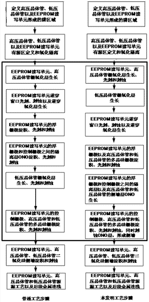
[0043] Hereinafter, the manufacturing method of the radiation-resistant EEPROM proposed by the present invention will be introduced in detail.

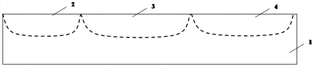
[0044] Such as diagram 2-1 As shown, P-type silicon 1 is used as the substrate material, its crystal orientation is , and the resistivity of the material is 15-25Ω·cm. The photolithographic definition of the well area is carried out through the mask plate: the ion implantation area of ​​the low-voltage transistor 2 well, the EEPROM memory unit 3 well, and the high-voltage transistor 4 well. Then ion implantation, glue removal, and high-temperature diffusion to form a low-voltage transistor well region, an EEPROM memory cell region well region, and a high-voltage transistor well region.

[0045] Such as Figure 2-2 As shown, an oxidation isolation is formed. Through the local oxidation process LOCOS or the shallow trench isolation process STI, multiple regions isolated by field oxides are formed on the P-type silicon 1, which are t...


PUM


Abstract

The invention provides a method for manufacturing an anti-radiation EEPROM. The memory includes devices: storage units and high and low voltage transistors of peripheral circuits. It is characterized in that the manufacturing method before the formation of the source and drain of each device is different from the ordinary manufacturing method. : The dielectric ONO layer used for the isolation between the floating gate and the control gate in the memory unit is used as the side wall of the high and low voltage transistor gate of the peripheral circuit at the same time, that is, the material of the side wall of the high and low voltage transistor gate is changed, by The silicon oxide film in the conventional manufacturing method is replaced by a composite film of silicon oxide and silicon nitride. The method of the present invention makes full use of the existing common manufacturing method, does not add additional process steps, only by adjusting the gate oxide growth sequence of the low-voltage transistor in the peripheral circuit, so as to ensure that the structure and electrical performance of the high-voltage and low-voltage transistor devices involved are consistent. Change, and improve the anti-radiation performance of the device, thereby improving the anti-radiation performance of the entire EEPROM. The method of the invention is suitable for mass production.

Description

technical field [0001] The invention relates to a semiconductor manufacturing method, in particular to a manufacturing method of EEPROM. Background technique [0002] Electrically Erasable Programmable Read-Only Memory-EEPROM (Electrically Erasable and Programmable Read-Only Memory) is a programmable read-only memory with a wide application market and development prospects. EEPROM can be erased and written directly with electrical signals, and has the advantages of fast speed and high integration, and is generally plug and play-Plug&Play. [0003] Since the development of microcomputers, the chip for storing BIOS has developed from the initial ROM (Read Only Memory), through PROM (Programmable ROM, programmable ROM), EPROM (Erasable Programmable ROM), and today's EEPROM (Electrically Erasable Programmable ROM, Electrically Erasable Programmable ROM) and Flash. The impetus for technological development and product upgrades can be seen from the product name, mainly from the ...

Claims


Application Information

Patent Timeline
Patent Type & Authority Patents(China)
IPC IPC(8): H01L27/11563H01L27/11573
CPCH01L21/823431H10B99/00
Inventor 杨冰奚鹏程
Owner SHANGHAI INTEGRATED CIRCUIT RES & DEV CENT
Why Eureka
Try Eureka