Semiconductor device and method for driving the same

a technology of semiconductor devices and semiconductor devices, applied in the direction of digital storage, capacitors, instruments, etc., can solve the problem that the semiconductor device can hold data for a long time, and achieve the effect of further improving the character of the semiconductor devi

Inactive Publication Date: 2011-08-18
SEMICON ENERGY LAB CO LTD
View PDF18 Cites 41 Cited by
  • Summary
  • Abstract
  • Description
  • Claims
  • Application Information

AI Technical Summary

Benefits of technology

[0029]Since the off-state current of a transistor including an oxide semiconductor is extremely small, stored data can be held for an extremely long period by using the transistor. In other words, refresh operation becomes unnecessary or the frequency of the refresh operation can be extremely low, which leads to a sufficient reduction in power consumption. Moreover, stored data can be held for a long period even when power is not supplied (note that a potential is preferably fixed).
[0030]Further, a semiconductor device according to the disclosed invention does not need high voltage for writing data, and deterioration of the element does not become a problem. For example, unlike a conventional non-volatile memory, it is not necessary to inject and extract electrons into and from a floating gate, and thus a problem such as deterioration of a gate insulating layer does not occur at all. That is, the semiconductor device according to the disclosed invention does not have a limit on the number of times of rewriting, which has been a problem of a conventional non-volatile memory, and thus has drastically improved reliability. Furthermore, since data is written by turning on or off the transistor, high-speed operation can be easily realized. Additionally, there is an advantage that operation for erasing data is not needed.
[0033]In the above semiconductor device, the potential converter circuit electrically connected to the gate of the transistor whose off-state current is sufficiently low is provided, whereby data can be successfully written to the node where the gate electrode of the transistor which can operate at sufficiently high speed, the source electrode or the drain electrode of the transistor whose off-state current is sufficiently low, and one electrode of the capacitor are electrically connected to one another. Therefore, characteristics of the semiconductor device can be further improved.

Problems solved by technology

When a semiconductor material which allows a sufficient reduction in off-state current of a transistor is used, the semiconductor device can hold data for a long time.

Method used


Image

  • Semiconductor device and method for driving the same
  • Semiconductor device and method for driving the same
  • Semiconductor device and method for driving the same

Examples


embodiment 1

[0060]In this embodiment, a basic circuit structure and operation of a semiconductor device according to one embodiment of the disclosed invention will be described with reference to FIGS. 1A-1, 1A-2, and 1B, FIG. 2, FIG. 3, FIG. 4, FIG. 5, and FIG. 6. Note that in each of the circuit diagrams, “OS” may be written beside a transistor in order to indicate that the transistor includes an oxide semiconductor.

1>

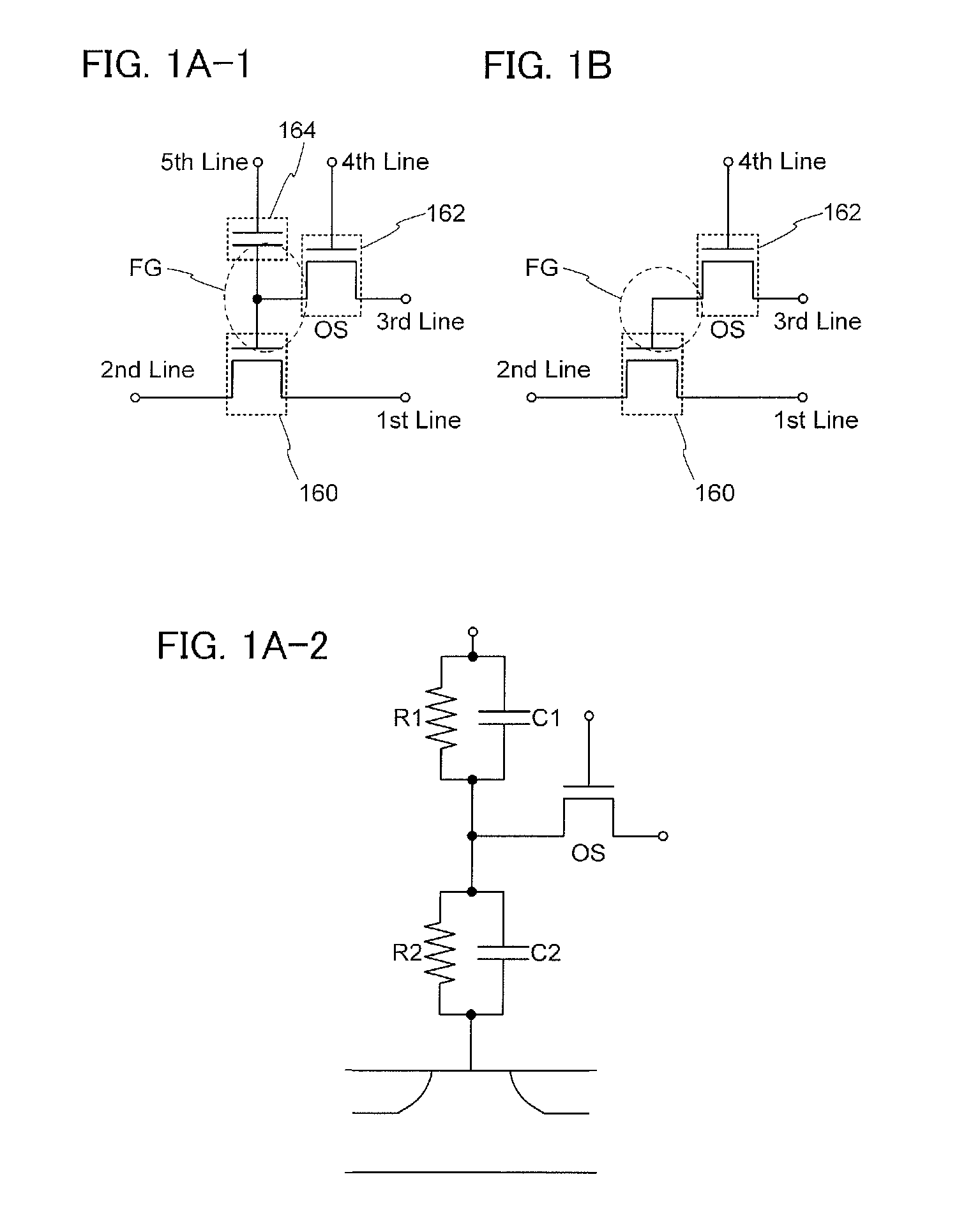
[0061]First, the most basic circuit structure and its operation will be described with reference to FIGS. 1A-1, 1A-2, and 1B. In the semiconductor device in FIG. 1A-1, a first wiring (a 1st line) and a source electrode (or a drain electrode) of a transistor 160 are electrically connected to each other, and a second wiring (a 2nd line) and the drain electrode (or the source electrode) of the transistor 160 are electrically connected to each other. In addition, a third wiring (a 3rd line) and a source electrode (or a drain electrode) of a transistor 162 are electrically connected t...

specific example

[0100]Next, a specific example of the potential converter circuit 1100 and operation of a semiconductor device using that will be described with reference to FIG. 3 and FIG. 4.

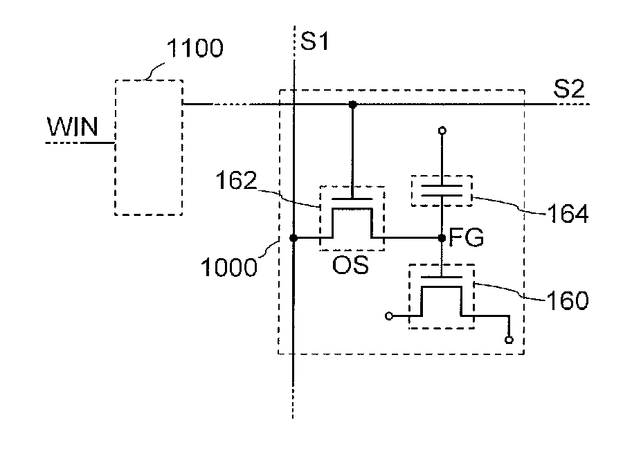
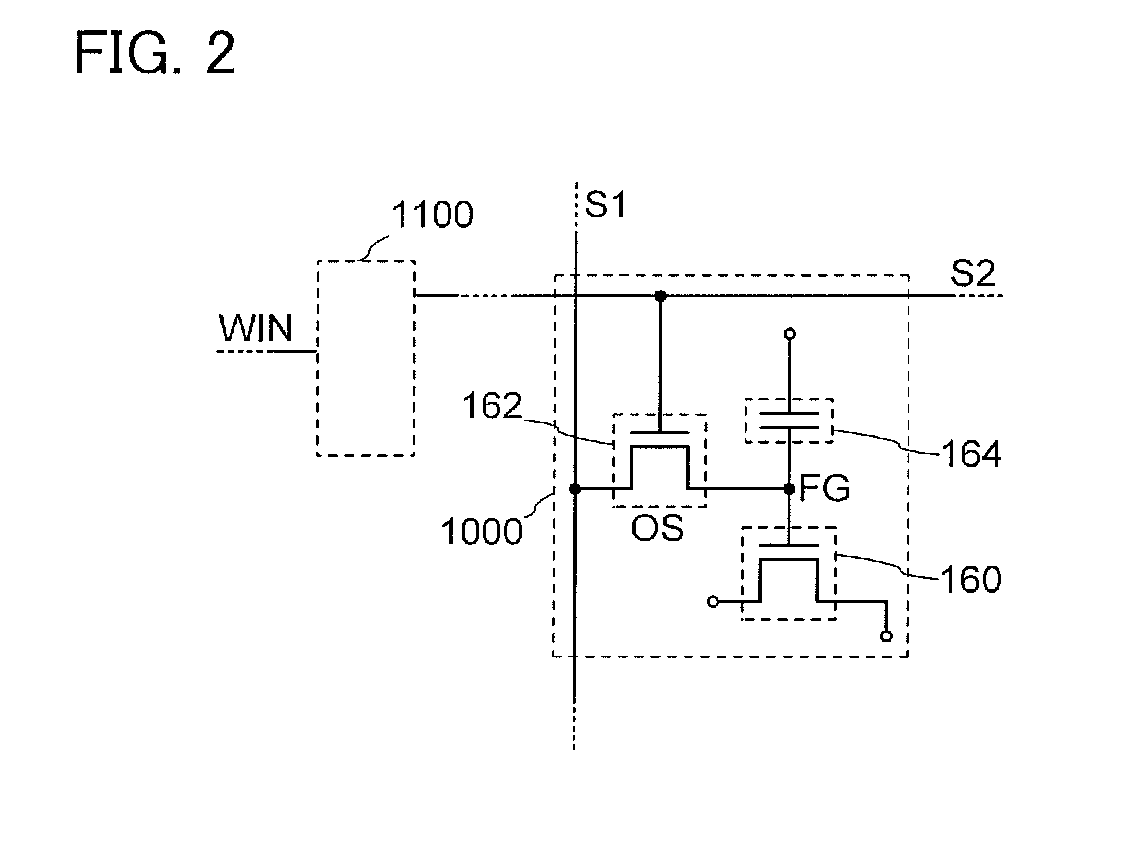
[0101]FIG. 3 illustrates an example of the potential converter circuit 1100 and the memory cell 1000. The potential converter circuit 1100 and the memory cell 1000 are connected to each other through the second signal line S2. Here, as a memory cell, the memory cell 1000 in FIG. 2 can be used.

[0102]The potential converter circuit 1100 includes a first wiring BT, a second wiring WIN, a third wiring CTRL, a transistor 201, a transistor 202, and a capacitor 200 (also referred to as a second capacitor).

[0103]Here, the second signal line S2, one electrode of the capacitor 200, and a source electrode (or a drain electrode) of the transistor 202 are electrically connected to one another. The other electrode of the capacitor 200 and a source electrode (or a drain electrode) of the transistor 201 are electrically conne...

embodiment 2

[0126]In this embodiment, a structure and a manufacturing method of a semiconductor device according to one embodiment of the disclosed invention will be described with reference to FIGS. 7A and 7B, FIGS. 8A to 8D, FIGS. 9A to 9C, FIGS. 10A to 10D, and FIGS. 11A to 11C.

[0127]FIGS. 7A and 7B illustrate an example of a structure of a semiconductor device. FIG. 7A illustrates a cross section of the semiconductor device, and FIG. 7B illustrates a plan view of the semiconductor device. Here, FIG. 7A illustrates a cross section taken along lines A1-A2 and B1-B2 in FIG. 7B. The semiconductor device illustrated in FIGS. 7A and 7B includes the transistor 160 including a first semiconductor material in a lower portion, and the transistor 162 including a second semiconductor material in an upper portion. Here, the first semiconductor material and the second semiconductor material are preferably different from each other. For example, the first semiconductor material may be a semiconductor mate...


PUM


Abstract

A semiconductor device includes a first signal line, a second signal line, a memory cell, and a potential converter circuit. The memory cell includes a first transistor including a first gate electrode, a first source electrode, a first drain electrode, and a first channel formation region; a second transistor including a second gate electrode, a second source electrode, a second drain electrode, and a second channel formation region; and a capacitor. The first channel formation region and the second channel formation region include different semiconductor materials. The second drain electrode, one electrode of the capacitor, and the first gate electrode are electrically connected to one another. The second gate electrode is electrically connected to the potential converter circuit through the second signal line.

Description

TECHNICAL FIELD[0001]The disclosed invention relates to a semiconductor device using a semiconductor element and a method for driving the semiconductor device.BACKGROUND ART[0002]Memory devices using semiconductor elements are broadly classified into two categories: a volatile device that loses stored data when not powered, and a non-volatile device that holds stored data even when not powered.[0003]A typical example of a volatile memory device is a dynamic random access memory (DRAM). A DRAM stores data in such a manner that a transistor included in a memory element is selected and charge is accumulated in a capacitor.[0004]Owing to the above principle, charge in the capacitor is lost when data in a DRAM is read out; thus, another writing operation is necessary every time data is read out. Moreover, since leakage current (off-state current) flows between a source and a drain of a transistor included in a memory element when the transistor is in an off state, charge flows into or ou...

Claims


Application Information

Patent Timeline
Patent Type & Authority Applications(United States)
IPC IPC(8): G11C5/06H01L29/12
CPCG11C11/405H01L27/11521H01L28/40H01L27/1225H01L27/1156H10B41/70H10B41/30H10B12/00
Inventor SAITO, TOSHIHIKOMATSUZAKI, TAKANORINAGATSUKA, SHUHEIINOUE, HIROKI
Owner SEMICON ENERGY LAB CO LTD
Why Eureka
Try Eureka