
Radiation image pickup apparatus and method of driving the same

a technology of image pickup and apparatus, which is applied in the direction of radioation control devices, instruments, television systems, etc., can solve the problem of difficulty in performing correct photoelectric conversion (image pickup) of radiation corresponding to incident energy

Inactive Publication Date: 2011-08-25
SONY SEMICON SOLUTIONS CORP
View PDF2 Cites 12 Cited by
  • Summary
  • Abstract
  • Description
  • Claims
  • Application Information

AI Technical Summary

Benefits of technology

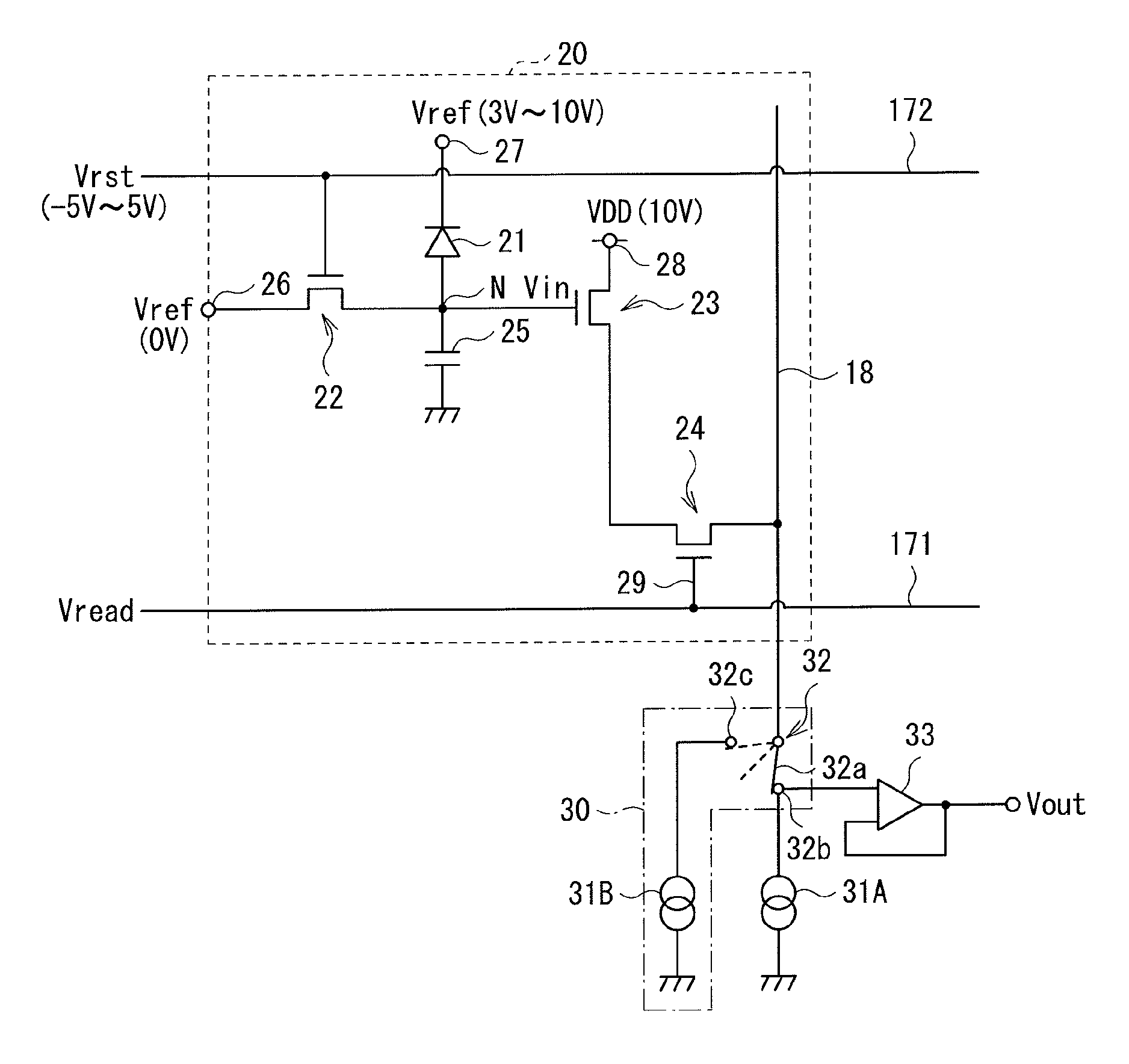
[0015]In the radiation image pickup apparatus or the method of driving a radiation image pickup apparatus according to the embodiment of the invention, at the time of non-measurement of radiation, a current path from the unit pixels is changed to the constant current source for annealing, and an annealing current flows through the pixel transistor. Therefore, heat is generated in a channel layer of the transistor to restore characteristics of the pixel transistor deteriorated by radiation.
[0016]In the radiation image pickup apparatus or the method of driving a radiation image pickup apparatus according to the embodiment of the invention, the constant current source for annealing is arranged, and at the time of non-measurement of radiation, the current path from the unit pixels is changed to the constant current source for annealing, and an annealing current flows through the pixel transistor; therefore, characteristics of the pixel transistor deteriorated by a crystal defect are restored, and accurate measurement corresponding to incident energy is allowed to be performed.
[0017]Other and further objects, features and advantages of the invention will appear more fully from the following description.

Problems solved by technology

However, in the radiation image pickup apparatus, there is an issue that X-rays or the like for measurement cause a crystal defect in a semiconductor layer of a pixel transistor and around an interface between the semiconductor and a gate insulating film or an interlayer insulating film.
When such a defect occurs, the threshold value (Vth) of the pixel transistor is changed (shifted), and characteristics vary from one transistor to another; therefore, it is difficult to perform correct photoelectric conversion (image pickup) of radiation corresponding to incident energy.

Method used


Image

  • Radiation image pickup apparatus and method of driving the same
  • Radiation image pickup apparatus and method of driving the same
  • Radiation image pickup apparatus and method of driving the same

Examples


first embodiment (

1. First Embodiment (radiation image pickup apparatus)

2. Descriptions of functions and effects

3. Modifications

4. Second Embodiment

FIRST EMBODIMENT

System Configuration

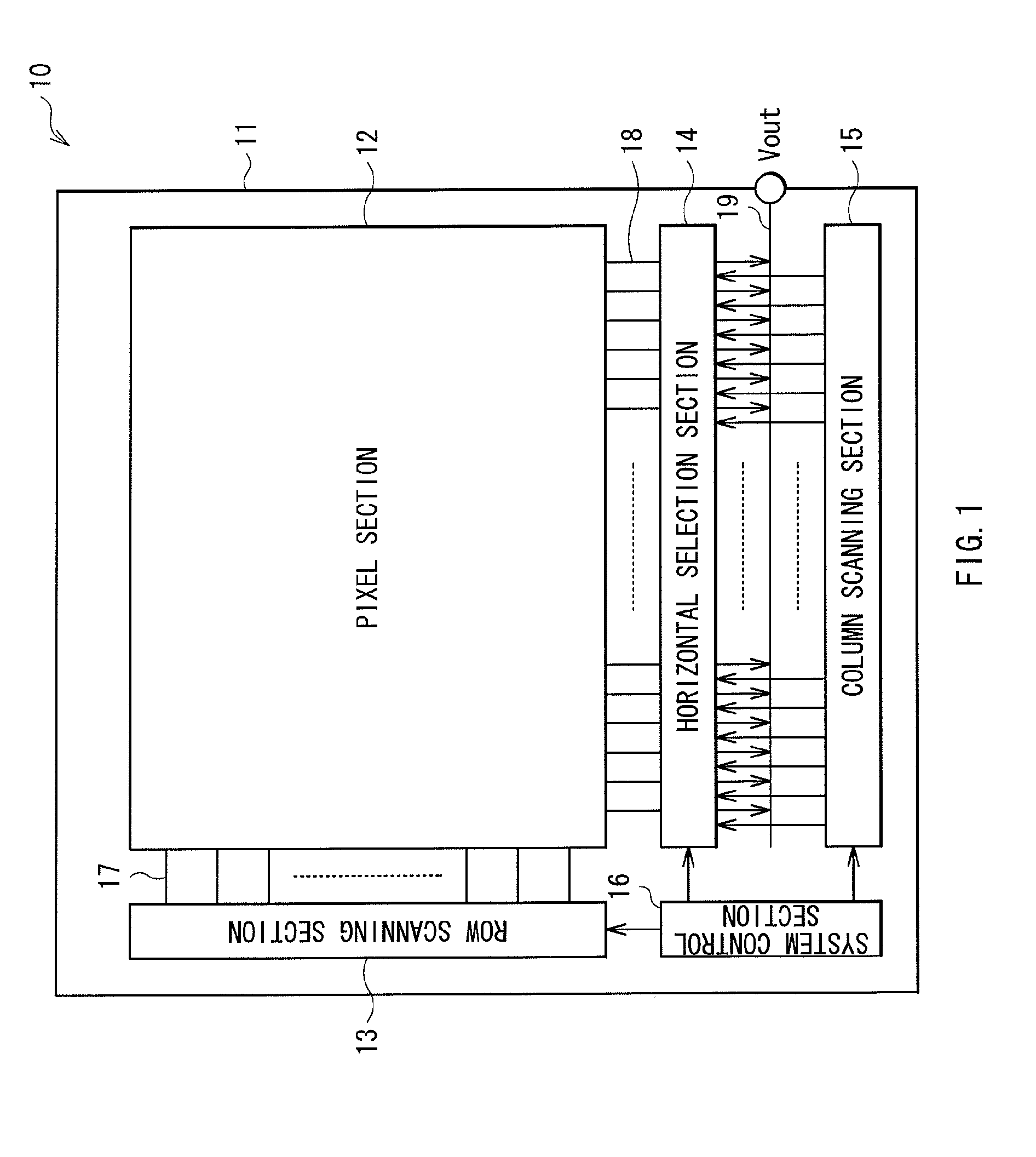
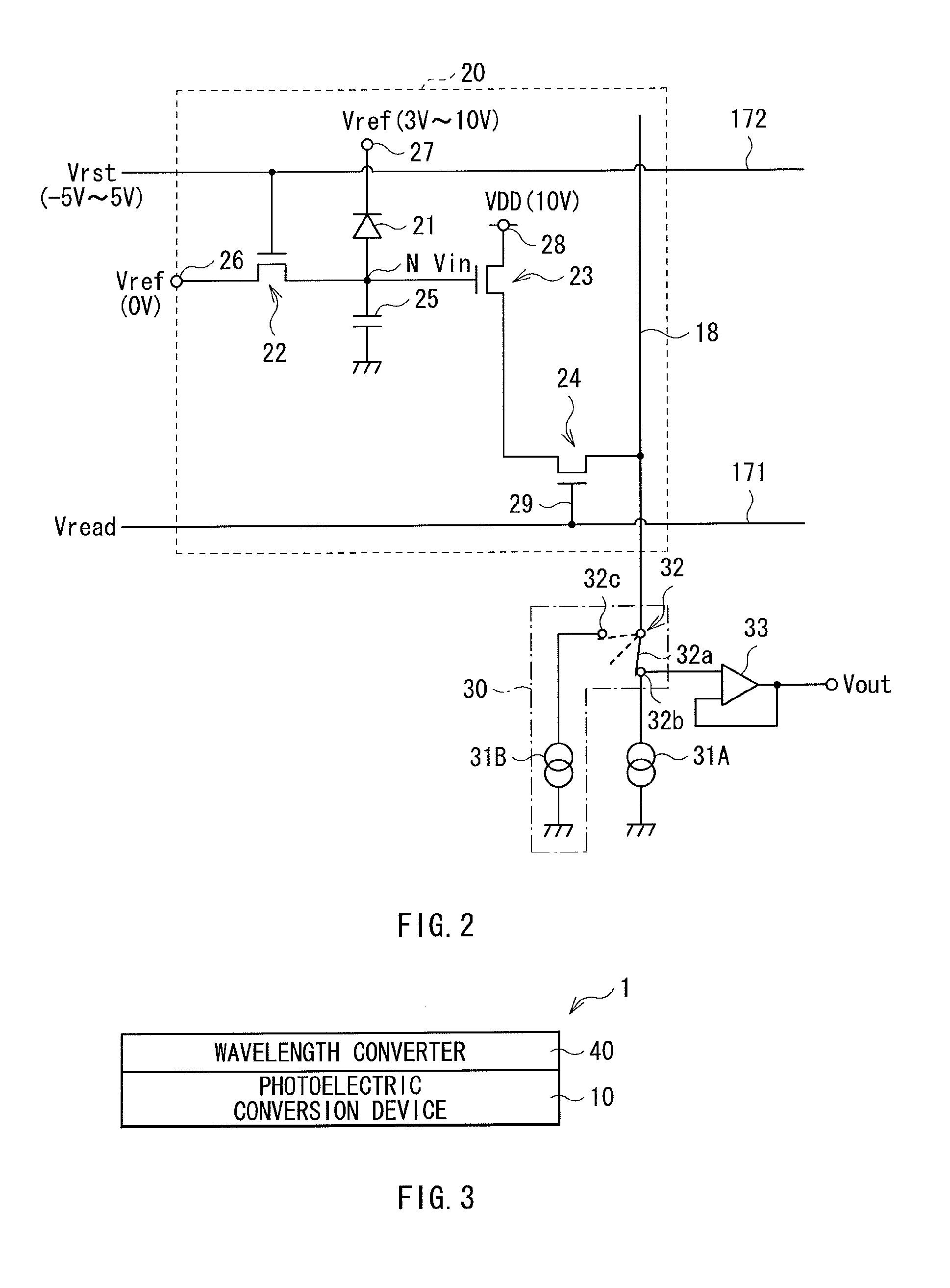
[0030]FIG. 1 illustrates a system configuration of a photoelectric conversion device 10 of a radiation image pickup apparatus according to a first embodiment of the invention. The radiation image pickup apparatus is configured by arranging a wavelength converter 40 (refer to FIG. 3) on the photoelectric conversion device 10, and reads information based on radiation by converting the wavelength of radiation represented by α-rays, β-rays, γ-rays or X-rays.

[0031]The photoelectric conversion device 10 includes a pixel section 12 on a substrate 11 made of an insulating material such as glass, and a peripheral circuit section (drive section) including, for example, a row scanning section (vertical drive section) 13, a horizontal selection section 14, a column scanning section (horizontal drive section) 15 and a system control...

second embodiment

[0073]In the above-described embodiment, an example in which the drive circuit of the pixel is configured of an active drive circuit is described, but the drive circuit of the pixel may be a passive drive circuit as illustrated in FIG. 10. Note that like components are denoted by like numerals as of the above-described embodiment and will not be further described.

[0074]In the embodiment, a unit pixel 90 is configured of the photoelectric conversion element 21, the capacity component 25 and a read transistor 91. The read transistor 91 is connected between the storage node N and the vertical signal line 18, and when the read transistor 91 turns on in response to the row scanning signal Vread, the read transistor 91 transmits a signal charge accumulated in the storage node N to the vertical signal line 18.

[0075]An end of the vertical signal line 18 is connected to an input terminal 92b of a measurement charge amplifier 92 having another internal terminal 92a connected to a ground. The ...


PUM


Abstract

A radiation image pickup apparatus allowed to restore a change in characteristics in a pixel transistors caused by radiation, and a method of driving the same are provided. The radiation image pickup apparatus includes: a pixel section including a plurality of unit pixels and generating an electrical signal based on incident radiation, each of the unit pixels including one or more pixel transistors and a photoelectric conversion element; a drive section for selectively driving the unit pixels of the pixel section; and a characteristic restoring section including a first constant current source for annealing and a selector switch for changing a current path from the unit pixels to the first constant current source at the time of non-measurement of the radiation, and allowing an annealing current to flow through the pixel transistor, thereby restoring characteristics of the pixel transistor.

Description

BACKGROUND OF THE INVENTION[0001]1. Field of the Invention[0002]The present invention relates to a radiation image pickup apparatus and a method of driving the same, and more specifically to a radiation image pickup apparatus (a radiation beam reader) reading information based on radiation by converting the wavelength of radiation represented by α-rays, β-rays, γ-rays or X-rays.[0003]2. Description of the Related Art[0004]In a radiation image pickup apparatus, a charge based on input information photoelectric-converted by a photoelectric conversion section is transferred to an external capacity, and the charge is converted into a signal voltage in the external capacity. When a charge is transferred from the capacity of the photoelectric conversion section to the external capacity to be converted into a signal voltage, a relatively large S / N is achievable.[0005]When a configuration in which a plurality of pixels are arranged is used, the length of a signal line reading signals from p...

Claims


Application Information

Patent Timeline
Patent Type & Authority Applications(United States)
IPC IPC(8): G01T1/24H01L29/04H01L27/146H04N25/00
CPCG01T1/2018H01L27/14676H04N5/378H04N5/374H04N5/2251H01L27/14658H04N25/76G01T1/20184H04N25/78H04N25/75
Inventor TANAKA, TSUTOMUTAKATOKU, MAKOTOYAMADA, YASUHIROITO, RYOICHI
Owner SONY SEMICON SOLUTIONS CORP
Learn More