
Semiconductor device and power conversion apparatus

a technology of semiconductor devices and power conversion apparatus, which is applied in the direction of semiconductor devices, solid-state devices, basic electric elements, etc., can solve the problems of undiscovered effective materials as alternatives to “high-temperature solder” and severely restricted use of lead, and achieve the effect of reducing characteristic defects and suppressing excessive stress

Active Publication Date: 2020-09-01
HITACHI POWER SEMICON DEVICE
View PDF30 Cites 0 Cited by
  • Summary
  • Abstract
  • Description
  • Claims
  • Application Information

AI Technical Summary

Benefits of technology

The present invention relates to improving the manufacturing process of semiconductor devices. It aims to prevent excessive stress from being applied to the gate wiring portion and protect the gate electrode from damage during the process of joining a metal plate onto a semiconductor chip with a gate structure. This invention can reduce defects and prevent cracks from occurring during the joining process.

Problems solved by technology

Meanwhile, the use of lead is severely restricted from the viewpoint of protecting the global environment, and development to use lead within such a restricted scope or to join an electrode or the like of a semiconductor device with a lead-free material has been advanced.
In particular, an effective material as an alternative to “high-temperature solder” has not yet been found.

Method used


Image

  • Semiconductor device and power conversion apparatus
  • Semiconductor device and power conversion apparatus
  • Semiconductor device and power conversion apparatus

Examples


example 1

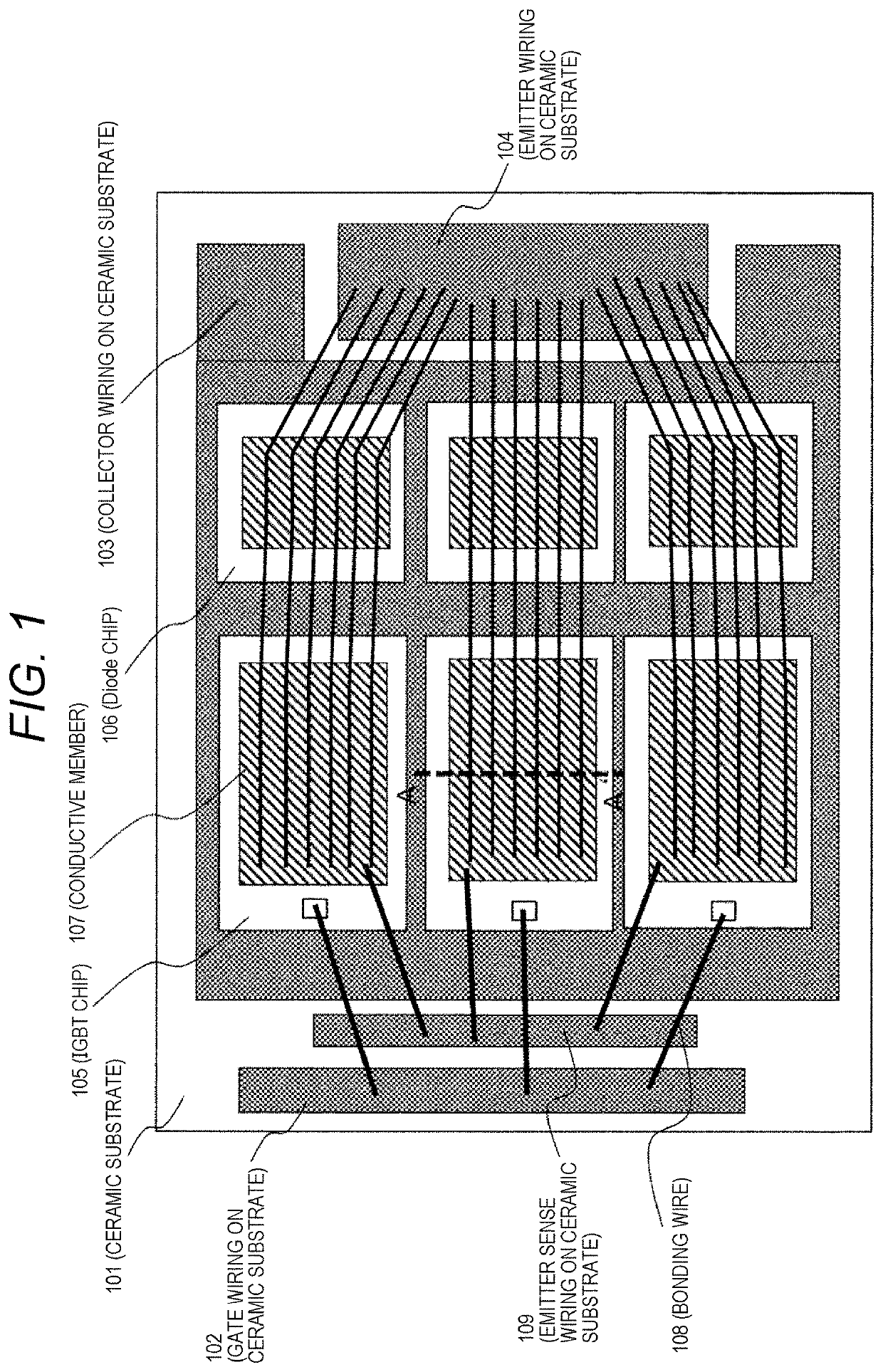
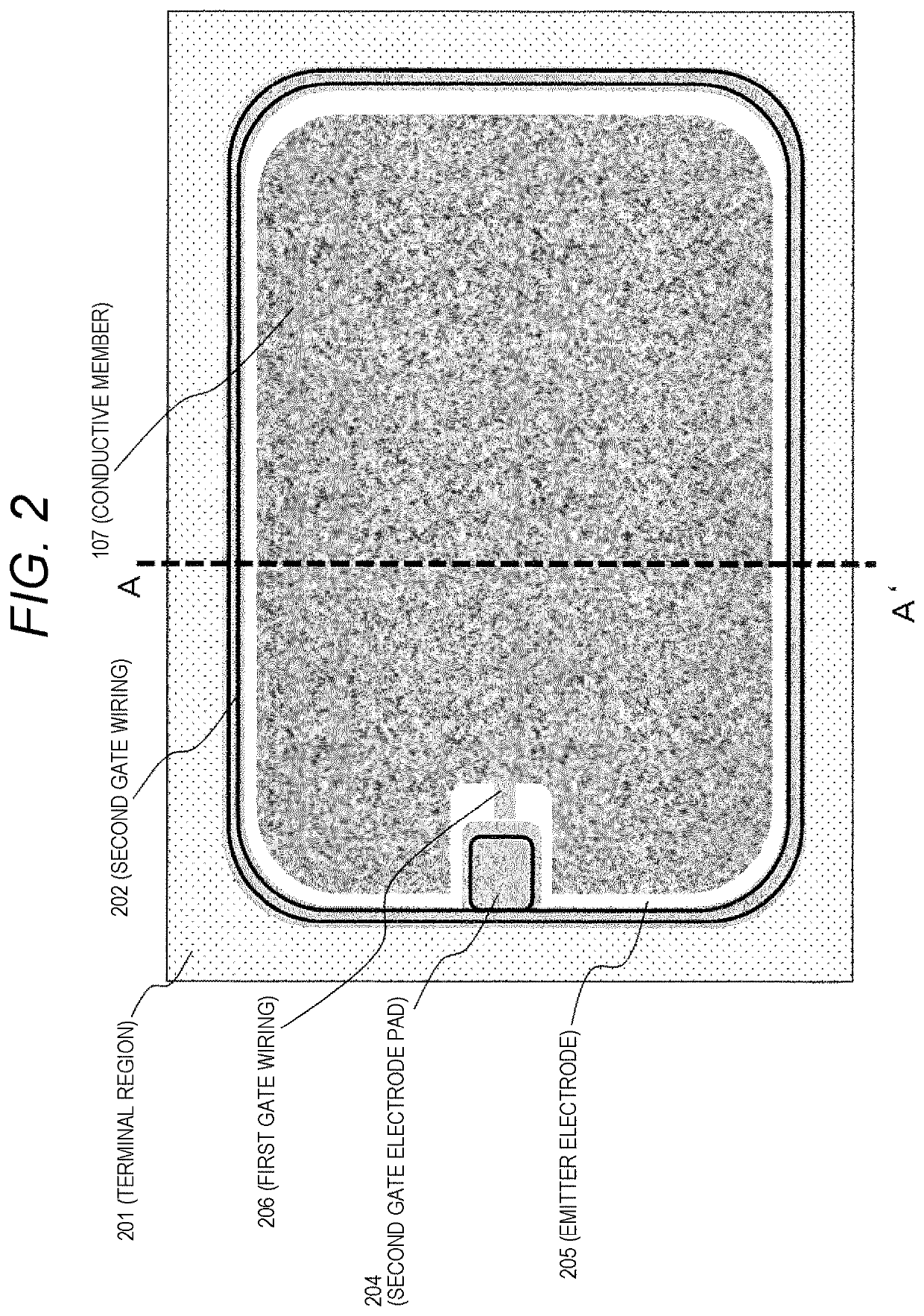
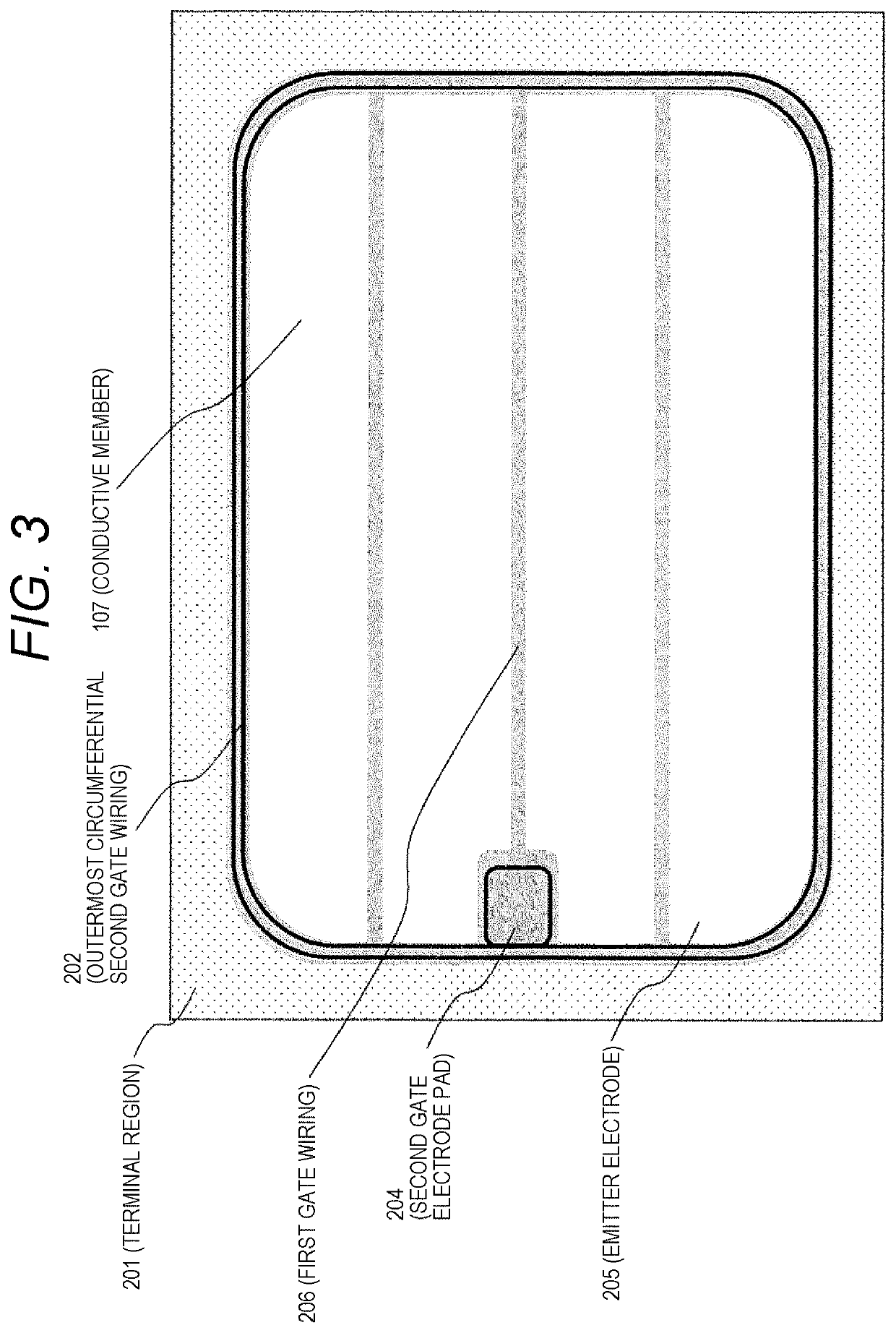
[0039]FIG. 1 is a top view of a semiconductor device according to Example 1 which is a first embodiment of the present invention. Further, FIG. 2 is a top view illustrating a mounting mode of a portion of the IGBT chip in the semiconductor device of FIG. 1. Further, FIG. 3 is a top view of the portion of the IGBT chip in the semiconductor device of FIG. 1. Further, FIG. 4 is a cross-sectional view illustrating a configuration of a cross section of the semiconductor device taken along a line A-A′ of FIG. 1.

[0040]The semiconductor device of this example is an example of the case of being applied to an IGBT module. Incidentally, the configuration of using a module in which an IGBT chip and a freewheel diode chip are mounted on a common collector wiring on a ceramic substrate as the semiconductor device will be described in this example, but the present invention is not limited to this configuration. It is possible to similarly apply a technical idea of the present invention even to, fo...

example 2

[0053]FIG. 12 is a layout diagram of a main part of a portion of the IGBT chip in a semiconductor device according to Example 2 which is a second embodiment of the present invention. Further, FIG. 13 is a bird's-eye view of a region E of FIG. 12. Parts having the same configurations as those of Example 1 will be denoted by the same reference numerals, and the overlapping part will not be described.

[0054]A feature of this example is that the active portion gate wiring 504 is buried in a trench portion to form a buried gate wiring 1201, which is different from Example 1. The other matters are common to those of Example 1. The buried gate wiring 1201 is formed in the same step as the trench gate 501, and the trench gate 501 and the buried gate wiring 1201 are connected in the trench. As compared with Example 1, it is possible to further reduce a difference in level between the active portion gate wiring 504 and the emitter electrode 205. Pressure at the time of connecting the conductiv...

example 3

[0055]FIG. 14 is a layout diagram of a main part of a portion of the IGBT chip in a semiconductor device according to Example 3 which is a third embodiment of the present invention. Further, FIG. 15 is a bird's-eye view of a region F of FIG. 14. Parts having the same configurations as those of Examples 1 and 2 will be denoted by the same reference numerals, and the overlapping part will not be described.

[0056]In the semiconductor device of this example, a gate is formed as a sidewall gate 1403 which is a type of a side gate structure, and the gate wiring 504 in the active portion is formed as a buried sidewall-type gate wiring 1402 and is connected to the sidewall gate 1403. This example is characterized by this point, and is different from Examples 1 and 2 in terms of this point. The other matters are common to those of Example 1.

[0057]A floating p layer 1202 is removed by providing a wide trench 1401. As a result, potential fluctuations of a gate due to influence of the floating p...


PUM

PropertyMeasurementUnit
particle diameteraaaaaaaaaa
particle sizeaaaaaaaaaa
pressureaaaaaaaaaa

Abstract

Provided is a semiconductor device in which, in a case where a metallic plate (a conductive member) is bonded by being sintered to a semiconductor chip having an IGBT gate structure, an excess stress is less likely to be generated in a gate wiring section of the semiconductor chip even when pressure is applied in a sinter bonding process, so that a characteristic failure is reduced. The semiconductor device according to the present invention is characterized by: being provided with a semiconductor chip having a gate structure represented by an IGBT; including first gate wiring and second gate wiring formed on the surface of the semiconductor chip; and including an emitter electrode disposed so as to cover the first gate wiring and a sintered layer disposed above the emitter electrode, wherein a multilayer structure formed by including at least the emitter electrode and the sintered layer on the surface of the semiconductor chip continuously exists over a range including an emitter electrode connecting contact and gate wiring regions.

Description

TECHNICAL FIELD[0001]The present invention relates to a semiconductor device characterized by a junction layer of an electrical junction (for example, a junction between a semiconductor element and a circuit member) in an electronic component, and particularly to a semiconductor device having a sintered junction layer and a power conversion apparatus using the same.BACKGROUND ART[0002]Semiconductor devices have been used in a wide range of fields such as system large scale integration (LSI), power conversion apparatuses, and control devices for hybrid vehicles. As such semiconductor devices, for example, one using “solder” or a “solder alloy” containing lead for electrical junction between an electrode terminal of an electronic component and an electrode terminal of a circuit pattern on a circuit board has been once the mainstream.[0003]Meanwhile, the use of lead is severely restricted from the viewpoint of protecting the global environment, and development to use lead within such a...

Claims


Application Information

Patent Timeline
Patent Type & Authority Patents(United States)
IPC IPC(8): H01L29/739H01L29/45H01L29/861H01L29/417H01L23/522
CPCH01L29/41708H01L29/45H01L23/522H01L29/861H01L29/7397H01L21/3205H01L21/768H01L25/07H01L25/18H01L29/417H01L29/78H01L2224/0603H01L2224/49111H01L2224/49175H01L29/7395H01L29/0696H01L29/4238H01L29/0619H01L29/402H02M7/003H02M7/5387H01L29/404H01L2224/48139H01L2224/48227H01L24/05H01L2224/0508H01L2224/03505H01L2224/48491H01L2224/05096H01L24/32H01L24/48H01L2224/8384H01L2224/04042H01L2224/04026H01L2224/32225H01L2224/73265H01L2224/05624H01L2924/00014H01L2924/00
Inventor FURUKAWA, TOMOYASUSHIRAISHI, MASAKIMORITA, TOSHIAKI
Owner HITACHI POWER SEMICON DEVICE
Learn More