Semiconductor device and semiconductor element

a semiconductor element and semiconductor technology, applied in the field of semiconductor devices, can solve the problems of reduced reliability, reduce reliability, and increase and achieve the effects of reducing reliability, reducing the probability of protective film being peeled, and increasing the stress applied to the semiconductor elemen

Active Publication Date: 2021-03-04
MITSUBISHI ELECTRIC CORP
View PDF0 Cites 1 Cited by
  • Summary
  • Abstract
  • Description
  • Claims
  • Application Information

AI Technical Summary

Benefits of technology

[0003]In a conventional semiconductor device, there has been a problem in that a semiconductor element receives a stress from a sealing resin due to a stress caused by a temperature cycle, a protective film on a surface of the semiconductor element is peeled off, and reliability thereof is reduced. In the semiconductor device having a structure disclosed in Japanese Patent Application Laid-Open No. 2001-274177, the stress applied to the semiconductor element is further increased, so that the probability that the protective film is peeled off is considered to be high. If the peeling of the protective film proceeds to, for example, a region that covers the gate wiring inside the terminal region, the gate wiring may be broken, and ultimately may result in a characteristic defect. In particular, in a semiconductor device on which a SiC semiconductor element is mounted, the Young's modulus of SiC is higher than that of Si; therefore, the stress applied to the protective film increases, and the peeling is more likely to progress. Also, even if the configuration disclosed in WO2013 / 137177 that improves the adhesion of the insulating layer is adopted, if the peeling cannot be completely suppressed, there are probabilities that the terminal region of the SiC semiconductor element having an intense electric field is exposed, electric discharge occurs from the peeled portion, and the breakdown voltage is reduced.

Problems solved by technology

In a conventional semiconductor device, there has been a problem in that a semiconductor element receives a stress from a sealing resin due to a stress caused by a temperature cycle, a protective film on a surface of the semiconductor element is peeled off, and reliability thereof is reduced.
If the peeling of the protective film proceeds to, for example, a region that covers the gate wiring inside the terminal region, the gate wiring may be broken, and ultimately may result in a characteristic defect.

Method used


Image

  • Semiconductor device and semiconductor element
  • Semiconductor device and semiconductor element
  • Semiconductor device and semiconductor element

Examples


embodiment 1

[0021]

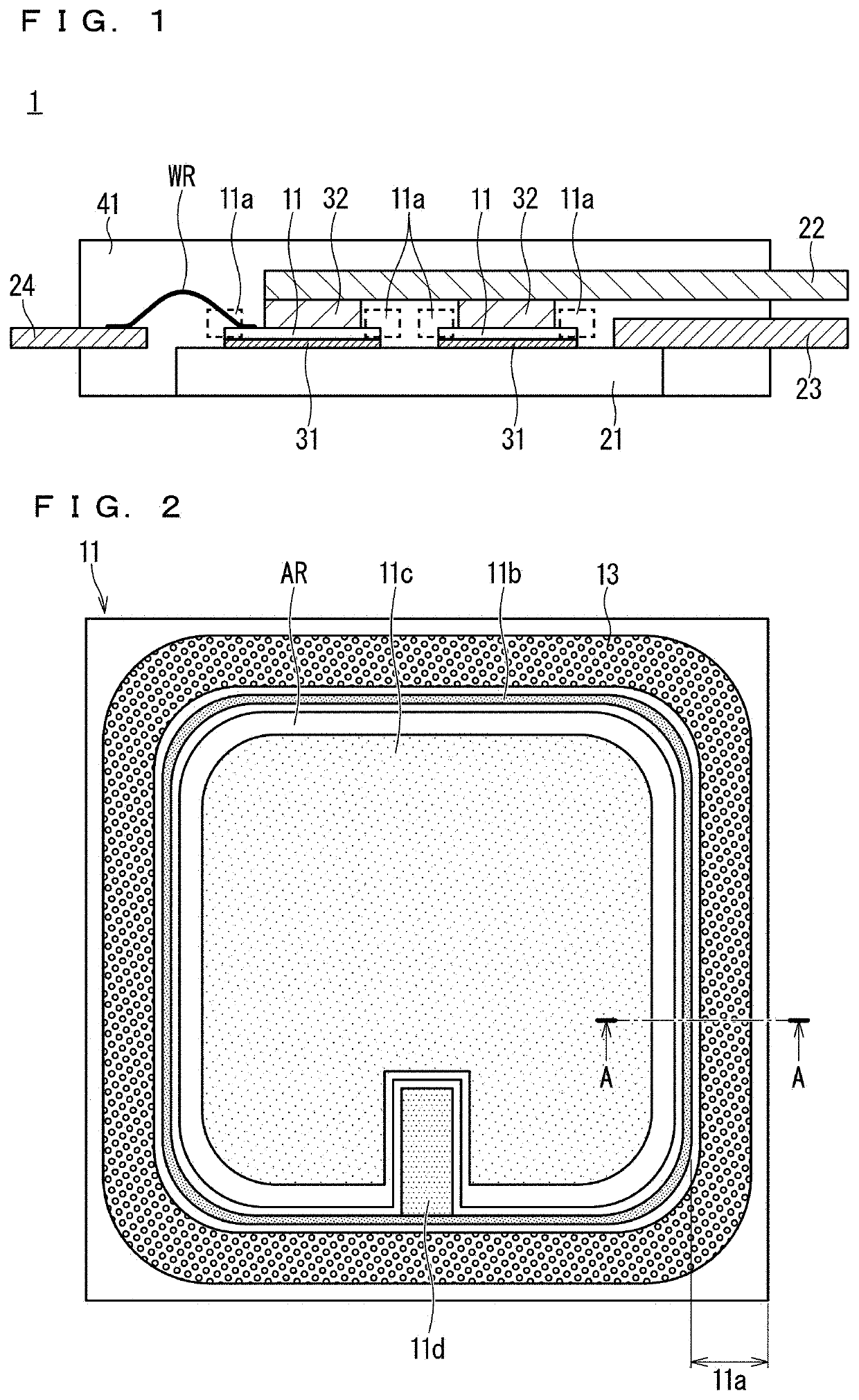
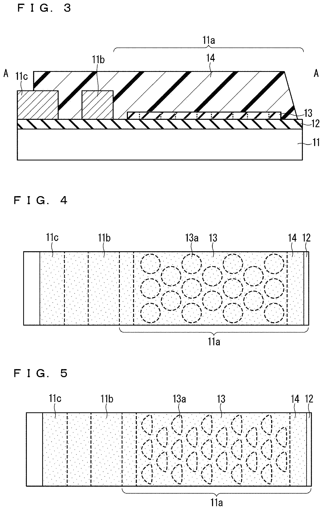
[0022]FIG. 1 is a cross-sectional view illustrating a configuration of a semiconductor device 1 according to Embodiment 1, and FIG. 2 is a plan view illustrating a configuration of semiconductor elements 11 mounted on the semiconductor device 1.

[0023]As illustrated in FIG. 1, the semiconductor device 1 includes a plurality of semiconductor elements 11 bonded on one main surface (upper surface) of a conductive substrate 21 via a bonding material 31 such as a solder material. In a semiconductor element 11, the lead frame 22 is bonded to the upper surface opposite to the lower surface bonded with the bonding material 31 via a bonding material 32 such as solder. The lead frame 22 is electrically connected to a source electrode (not shown) on the upper surface of the semiconductor elements 11, and one end of the lead frame 22 projects outside the semiconductor device 1.

[0024]One end of an external terminal 23 is connected to an edge portion of the upper surface of the conductive su...


PUM

PropertyMeasurementUnit
thicknessaaaaaaaaaa
widthaaaaaaaaaa
semiconductoraaaaaaaaaa

Abstract

the semiconductor device includes a substrate, a semiconductor element bonded to the substrate, and a sealing resin sealing at least a part of the substrate and the semiconductor element, in which the semiconductor element includes an active region through which a main current flows in an ON state of the semiconductor element, a terminal region surrounding the active region, an anchor film provided on an insulating film of the terminal region, and a protective film covering at least the terminal region including the anchor film, and the anchor film consists of a material different from the insulating film and has a plurality of openings provided discretely.

Description

BACKGROUND OF THE INVENTIONField of the Invention[0001]The present invention relates to a semiconductor device, in particular, to a semiconductor device in which a semiconductor element is sealed with a resin, in which peeling of a protective film for protecting the semiconductor element is suppressed.Description of the Background Art[0002]Japanese Patent Application Laid-Open No. 2004-165406 discloses a semiconductor device in which a semiconductor element is sealed with a curable resin such as an epoxy resin. Further, Japanese Patent Application Laid-Open No. 2001-274177 discloses a semiconductor device in which electrode members are bonded to a front side and a back side of a semiconductor element, and at least a part of the electrode member and the semiconductor element are covered with a sealing resin. In recent years, in order to be able to cope with further loss reduction and high-temperature operation, SiC semiconductor elements consist of silicon carbide (SiC) have been dev...

Claims


Application Information

Patent Timeline
Patent Type & Authority Applications(United States)
IPC IPC(8): H01L23/31H01L29/16H01L23/29H01L23/16H01L23/00
CPCH01L23/3135H01L29/1608H01L23/562H01L23/16H01L23/293H01L23/3157H01L23/3171H01L23/3142H01L2224/48091H01L2224/48247H01L2224/0603H01L2224/73265H01L2924/181H01L2224/33181H01L2224/45124H01L2224/45147H01L2224/45015H01L24/45H01L24/48H01L24/05H01L2224/02166H01L2224/04026H01L2224/04042H01L24/06H01L2224/02235H01L2224/02255H01L2224/92247H01L2224/83801H01L2224/48472H01L2224/29101H01L2224/29111H01L2924/15747H01L2224/29339H01L2224/29347H01L2224/8384H01L24/29H01L24/83H01L24/85H01L2224/06051H01L2224/0555H01L2224/05552H01L2224/05553H01L24/40H01L2224/40137H01L2224/84801H01L2224/8484H01L24/84H01L24/33H01L2224/04034H01L2224/73221H01L2924/00014H01L2924/00012H01L2924/2076H01L2224/32245H01L2924/014
Inventor NAKATA, YOSUKE
Owner MITSUBISHI ELECTRIC CORP
Why Eureka
Try Eureka