

Optical element mount for lithographic apparatus
- Summary
- Abstract
- Description
- Claims
- Application Information
AI Technical Summary
Benefits of technology
Problems solved by technology
Method used
Image

Examples
Embodiment Construction
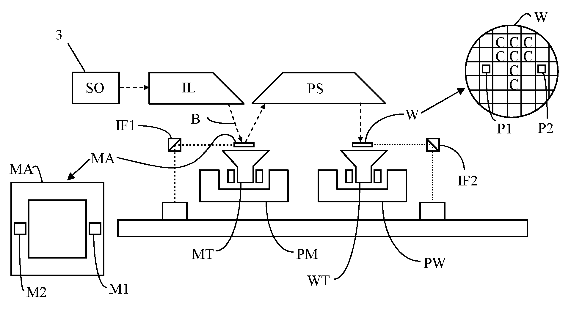
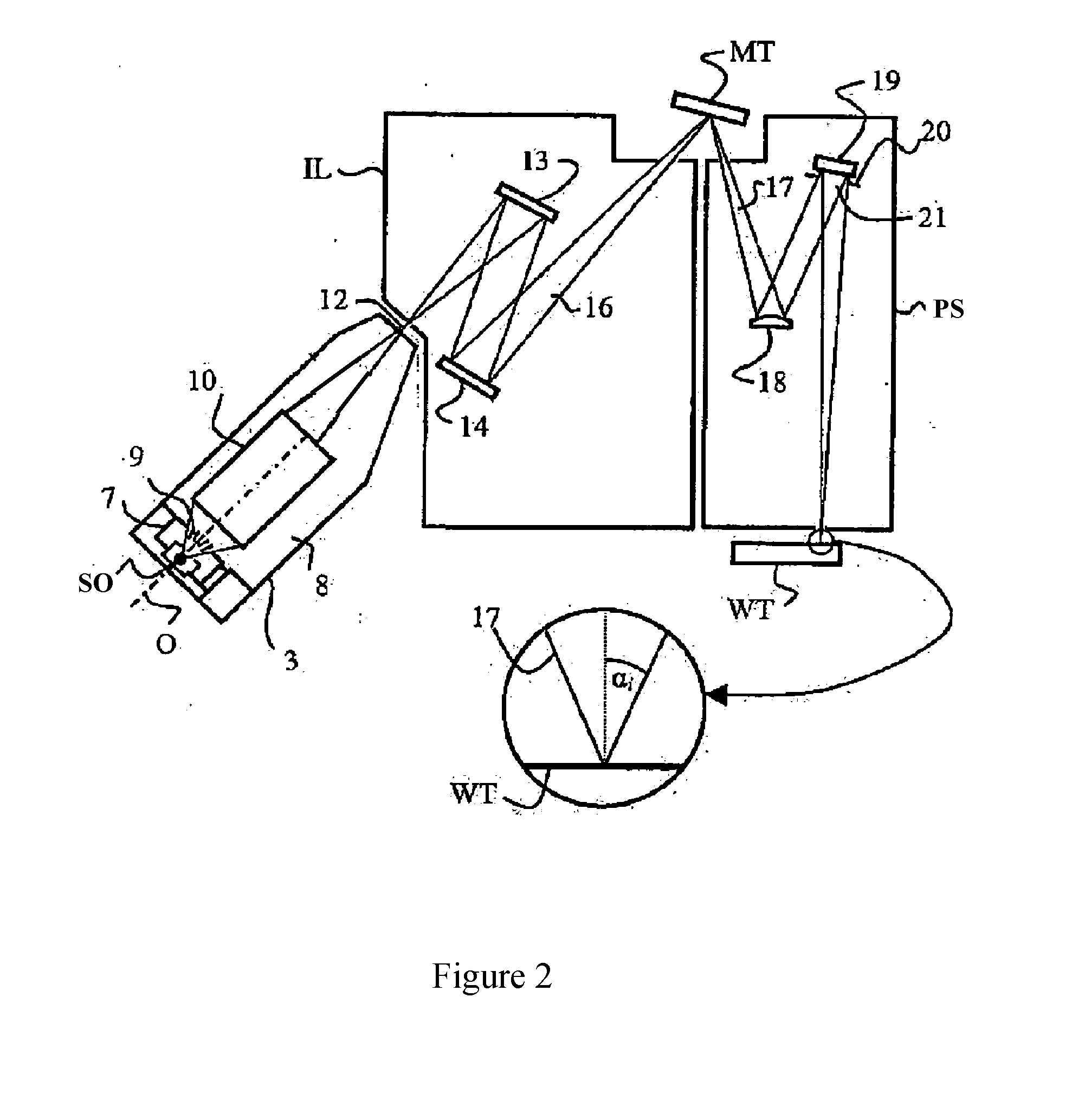
FIG. 1 schematically depicts an embodiment of a lithographic apparatus, that can be or include an embodiment of the invention. The apparatus includes an illumination system (illuminator) IL configured to condition a radiation beam B (e.g. EUV radiation); a support structure or patterning device support (e.g. a mask table) MT constructed to support a patterning device (e.g. a mask or a reticle) MA and connected to a first positioner PM configured to accurately position the patterning device; a substrate table (e.g. a wafer table) WT constructed to hold a substrate (e.g. a resist-coated wafer) W and connected to a second positioner PW configured to accurately position the substrate; and a projection system (e.g. a reflective projection lens system) PS configured to project a pattern imparted to the radiation beam B by patterning device MA onto a target portion C (e.g. including one or more dies) of the substrate W.
The illumination system may include various types of optical components...
PUM
 Abstract
Description
Claims
Application Information