
Integrally Molded Die And Bezel Structure For Fingerprint Sensors And The Like

Inactive Publication Date: 2011-09-08
APPLE INC
View PDF12 Cites 24 Cited by
  • Summary
  • Abstract
  • Description
  • Claims
  • Application Information

AI Technical Summary

Benefits of technology

[0011]By encasing both the bezel and the sensor die in the encapsulation structure, those elements may be brought closer together than heretofore possible. In addition, the encapsulation structure physically protects the bezel and sensor die, and in particular maintains the spacing therebetween, in a fashion not possible by currently known device designs.
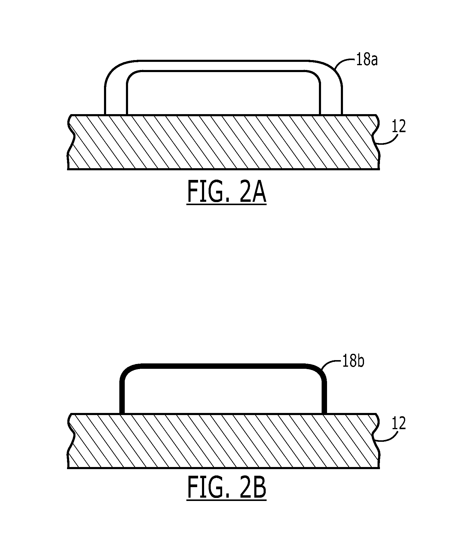
[0013]The molding of the bezel and sensor die may be such that the top surface of the bezel and the top surface of the sensor die are coplanar. Alternatively, the plane of the top surface of the bezel and the top surface of the sensor die may be generally parallel, but not coplanar, such that the plane of the top surface of the bezel is slightly above the plane of the top surface of the sensor die. In this case, the top surface of the bezel may protrude slightly above the encapsulation material, for example to improve physical contact therewith by a user's finger. Also in this case, it may be desirable to provide the bezel with a slightly rounded cross-section for user comfort, for device robustness, to avoid the buildup of contaminants at the bezel edge, etc.

Problems solved by technology

However, certain fingerprint sensor designs include thin protective overcoats over the sensor surface to protect the sensors from physical and environmental damage, wear, etc.
As the number of discrete elements and manufacturing steps increase, manufacturing cost increases and the potential for faulty or inaccurate assembly that negatively affects product consistency and yield losses increase.
Discrete element sub-assembly is also a more time consuming process than integrated manufacturing.
As in the general art of IC production, there is significant, ongoing commercial pressure to reduce cost, number of components, and number and complexity of manufacturing steps, and size of the completed structure.

Method used


Image

  • Integrally Molded Die And Bezel Structure For Fingerprint Sensors And The Like
  • Integrally Molded Die And Bezel Structure For Fingerprint Sensors And The Like
  • Integrally Molded Die And Bezel Structure For Fingerprint Sensors And The Like

Examples


first embodiment

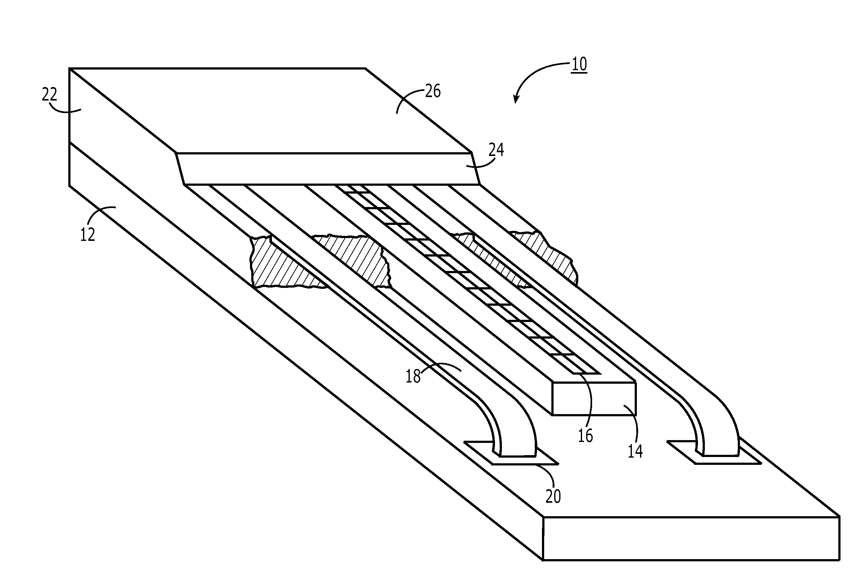
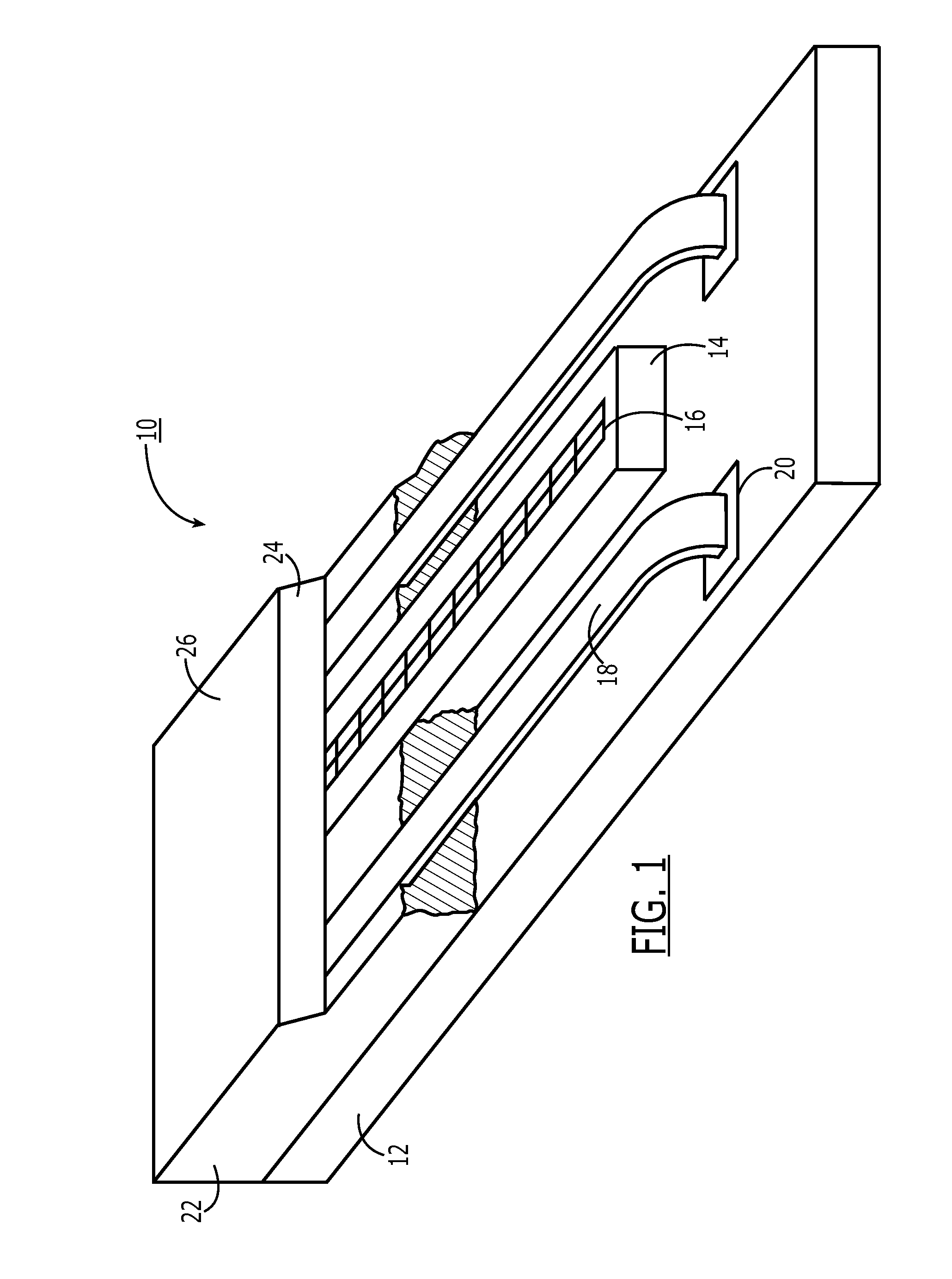
[0027]With reference first to FIG. 1, there is shown therein a partial cut-away perspective view of a biometric sensor assembly 10 according to a Assembly 10 comprises a substrate 12, which may be a printed circuit board (PCB), ceramic body, or similar structure having formed thereon, and possibly in layers thereof, interconnection leads (not shown). Secured to substrate 12 in a die-receiving region is sensor integrated circuit, or die, 14. Die 14 is typically a semiconductor body have one or more layers formed thereon, including electrical devices such as transistors, capacitors, interconnections and the like formed photolithographically or by other semiconductor manufacturing processes. Specifically, die 14 has formed thereon a two-dimensional array 16 of sensor pixels and sensing circuitry. Die 14 may be physically connected to substrate 12 by an adhesive between the bottom side of die 14 and the top side of substrate 12, and electrically connected by a plurality of wirebonds fr...

embodiment 46

[0038]In embodiment 46 shown in FIG. 7C, the plane of the top surface of die 14 and the plane of the top surface of bezels 18 are not coplanar. The plane of the top surface of bezels 18 is slightly above the plane of the top surface of die 14 (by distance d). In this case, the top surface of bezels 18 may protrude slightly above the encapsulation material 22, for example to improve physical contact therewith by a user's finger (not shown). Also in this case, it may be desirable to provide bezels 18 with a slightly rounded top surface (shown in cross-section in FIG. 7C) or corners for user comfort, for device robustness, to avoid the buildup of contaminants at the bezel edge, etc.

[0039]In embodiment 80 shown in FIGS. 8A and 8B, a substrate 82 has physically connected thereto a die 84. The connection may also be electrical, as described above. Die 84 has formed therein a sensor region 86, also as described above. A bezel 88 is also physically, and optionally electrically, connected to...


PUM


Abstract

A biometric sensor device, such as a fingerprint sensor, comprises a substrate to which is mounted a die on which is formed a sensor array and at least one conductive bezel. The die and the bezel are encased in a unitary encapsulation structure to protect those elements from mechanical, electrical, and environmental damage, yet with a portion of the sensor array and the bezel exposed or at most thinly covered by the encapsulation or other coating material structure.

Description

CROSS-REFERENCE TO RELATED APPLICATIONS[0001]The present disclosure is related to and incorporates by reference application for U.S. letters patent Ser. No. ______, attorney docket number UPE 09-03, titled “Biometric Sensor Assembly with Integrated Visual Indicator”.BACKGROUND[0002]The present disclosure is related to integrated circuit packaging, and more specifically to methods and apparatus for integrally molding a die and one or more bezel structures, with portions of each exposed or at most thinly covered, for fingerprint sensors and the like.[0003]One relatively common biometric sensing device today is the fingerprint sensor. These devices are used in controlling access to electronic devices such as computers and mobile phones, safes, buildings, vehicles, etc. by scanning a user's fingerprint and comparing it to an authenticating set of fingerprint images. If the proffered (live) fingerprint to be authenticated matches one within a set of pre-enrolled authorized fingerprints, ...

Claims


Application Information

Patent Timeline
IPC IPC(8): H01L23/31
CPCG06K9/0002G06K9/00053H01L27/20H01L2224/48091G06V40/1306H01L2924/00014G06V10/10G06V40/1329H10N39/00
Inventor BOND, ROBERTKRAMER, ALANGOZZINI, GIOVANNI
Owner APPLE INC
Learn More