Organic-inorganic hybrid perovskite surface interface treatment method, material and application

A processing method and perovskite technology, applied in the direction of organic semiconductor devices, electric solid devices, semiconductor devices, etc., can solve the problems that additive engineering has not been widely used, the dosage and the preparation process are sensitive, and achieve the improvement of device interface electrical and Physical contact, improved device performance and stability, and low cost effects

Active Publication Date: 2022-05-06
GUILIN UNIV OF ELECTRONIC TECH
View PDF4 Cites 1 Cited by
  • Summary
  • Abstract
  • Description
  • Claims
  • Application Information

AI Technical Summary

Problems solved by technology

Additive engineering is not widely used because device performance is very sensitive to additive dosage and fabrication process

Method used


Image

  • Organic-inorganic hybrid perovskite surface interface treatment method, material and application
  • Organic-inorganic hybrid perovskite surface interface treatment method, material and application
  • Organic-inorganic hybrid perovskite surface interface treatment method, material and application

Examples


Embodiment 1

[0056] Such as Figure 7 As shown, an organic-inorganic hybrid perovskite surface interface treatment method, its preparation process is as follows:

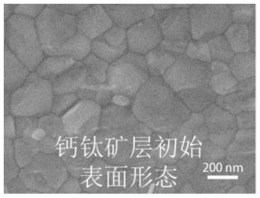
[0057] Step 1). Prepare an organic-inorganic hybrid perovskite film, wherein the perovskite layer material in the organic-inorganic hybrid perovskite film is methylamine lead iodide (MAPbI 3 );

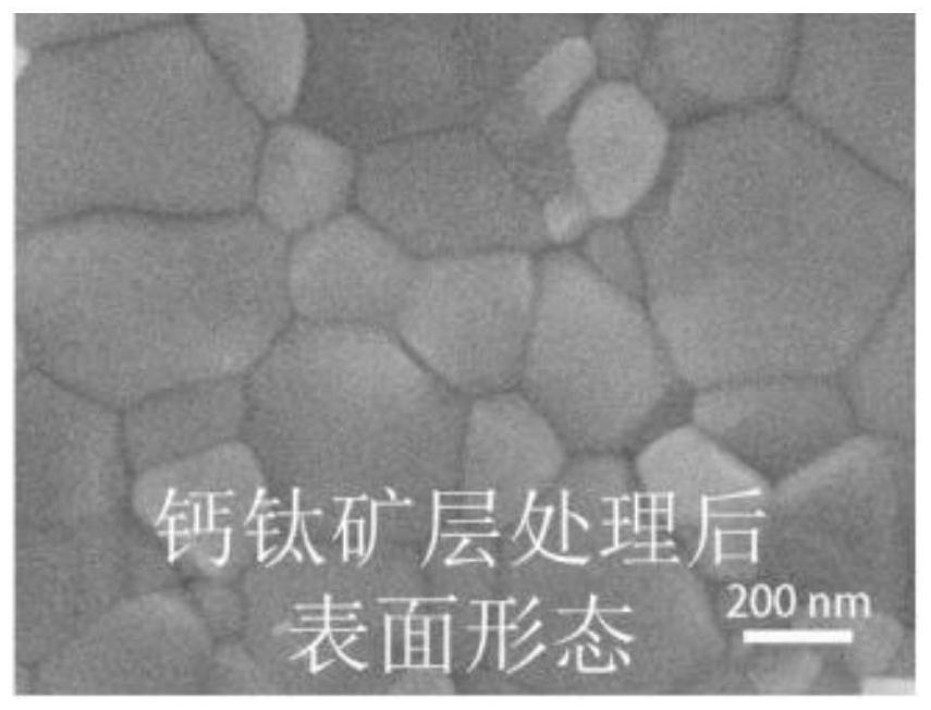
[0058] The surface of the organic-inorganic hybrid perovskite film prepared in step 2) is treated with N-benzyloxycarbonyl-D-valine material, the purity of N-benzyloxycarbonyl-D-valine material is 98%, soluble in Chlorobenzene solution, the treatment solution concentration is 0.05mg / mL, and the treatment method is spin coating;

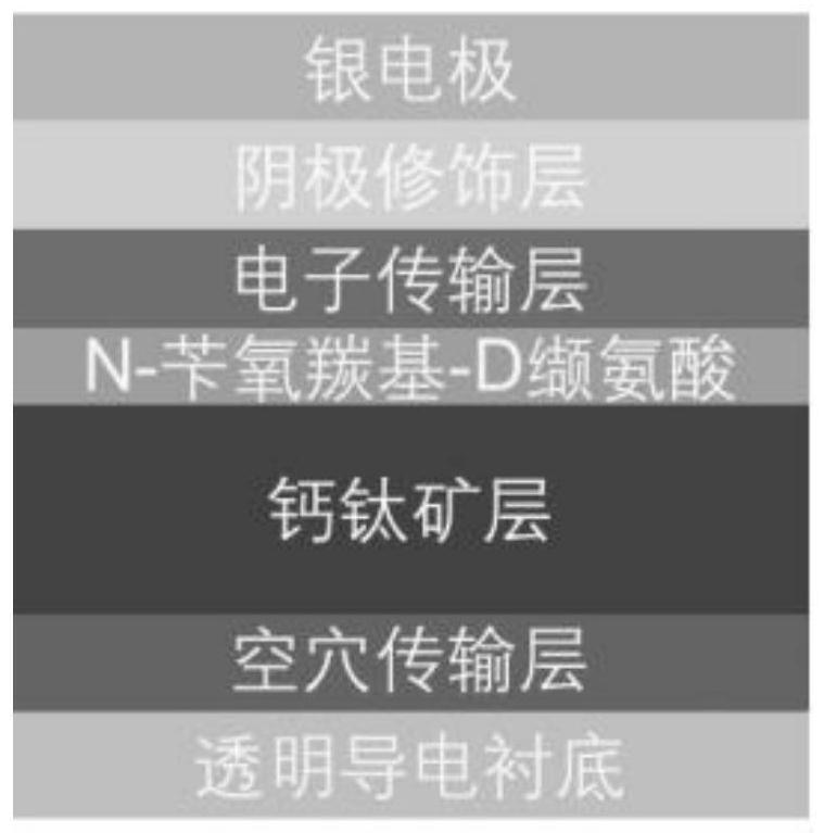
[0059] Such as figure 1 As shown, the prepared perovskite film is applied in an inverted perovskite solar cell, and its preparation process is as follows:

[0060] Step 1). Spin-coat the hole transport layer on the transparent conductive substrate, the thickness of the hole transport layer is 5nm, heat trea...

Embodiment 2

[0066] A method for treating the surface and interface of an organic-inorganic hybrid perovskite, the preparation method of which is the same as that of Comparative Example 1.

[0067] The prepared perovskite thin film is applied in an inverted perovskite solar cell, and its preparation process is as follows:

[0068] Step 1). Spin-coat the hole transport layer on the transparent conductive substrate, the thickness of the hole transport layer is 5nm, heat treatment at a temperature of 100 ℃, the treatment time is 10 minutes, the transparent conductive substrate is fluorine-doped oxide Tin (FTO), the hole transport layer is poly[bis(4-phenyl)(2,4,6-trimethylphenyl)amine](PTAA);

[0069] Step 2). Spin-coat the perovskite layer with the perovskite film on the hole transport layer described in step 1), the thickness of the perovskite layer is 300nm, heat treatment at 100°C;

[0070] Step 3). The electron transport layer is spin-coated on the surface of the perovskite layer with a...

Embodiment 3

[0074] A method for treating the surface and interface of organic-inorganic hybrid perovskite, the preparation process of which is as follows:

[0075]Step 1). Prepare an organic-inorganic hybrid perovskite film, wherein the perovskite layer material in the organic-inorganic hybrid perovskite film is cesium-doped formamidine methylamine lead-iodine-bromine blended perovskite (Cs x (MA y FA 1-y ) 1-x Pb(I z Br 1-z ) 3 ;1>x>0, 1>y>0, 1>z>0);

[0076] The surface of the organic-inorganic hybrid perovskite film prepared in step 2) is treated with N-benzyloxycarbonyl-D-valine material, the purity of N-benzyloxycarbonyl-D-valine material is 98%, soluble in Chlorobenzene solution, the treatment solution concentration is 0.10mg / mL, and the treatment method is slit coating;

[0077] Step 3). Appropriate heat treatment is performed on the organic-inorganic hybrid perovskite treated in step 2). The heat treatment method is infrared heating. The heat treatment temperature is 100 de...


PUM


Abstract

The invention provides an organic-inorganic hybrid perovskite surface interface treatment method, a material and application. The method comprises the following steps: 1) preparing an organic-inorganic hybrid perovskite thin film; (2) treating the surface of the organic hybrid perovskite thin film prepared in the step (1) by adopting an N-carbobenzoxy-D valine material; and 3) carrying out proper heat treatment on the organic-inorganic hybrid perovskite thin film treated by the N-carbobenzoxy-D-valine material obtained in the step 2). The effect of adjusting the quality of the whole perovskite thin film can be achieved through the simple and convenient surface treatment method, and the method is simple in process, low in cost, green, free of pollution and suitable for large-scale production and application.

Description

technical field [0001] The invention relates to the technical field of photovoltaic cells, in particular to an organic-inorganic hybrid perovskite surface and interface treatment method, material and application. Background technique [0002] With the development of society, people's demand for energy is increasing, and at the same time they are facing problems such as environmental pollution and resource scarcity. Therefore, people need to find new energy sources to replace traditional energy sources. Solar energy is favored by people as the most widely distributed and largest energy source, and solar cells can convert solar energy into the most widely used electrical energy. After years of development, solar cells have developed to the third generation. The first and second generations cannot be mass-produced and applied due to factors such as high cost and difficulty in manufacturing. The third generation of solar cells has low cost, high efficiency and reliability. It i...

Claims


Application Information

Patent Timeline
Patent Type & Authority Applications(China)
IPC IPC(8): H01L51/48H01L51/42H01L51/46
CPCH10K71/12H10K71/421H10K85/111H10K85/113H10K30/10H10K2102/00Y02E10/549
Inventor 熊健刘乃赫梁伟忠刘伟之戴骏乾张潞许云飞黄瑜张哲泠张坚
Owner GUILIN UNIV OF ELECTRONIC TECH
Why Eureka
Try Eureka