Variable resistance nonvolatile storage device
a non-volatile storage and variable resistance technology, applied in semiconductor devices, digital storage, instruments, etc., can solve the problems of large voltage drop caused by line resistance, and achieve the effect of improving yield and increasing reading speed of memory cells
- Summary
- Abstract
- Description
- Claims
- Application Information
AI Technical Summary
Benefits of technology
Problems solved by technology
Method used
Image

Examples
embodiment 1
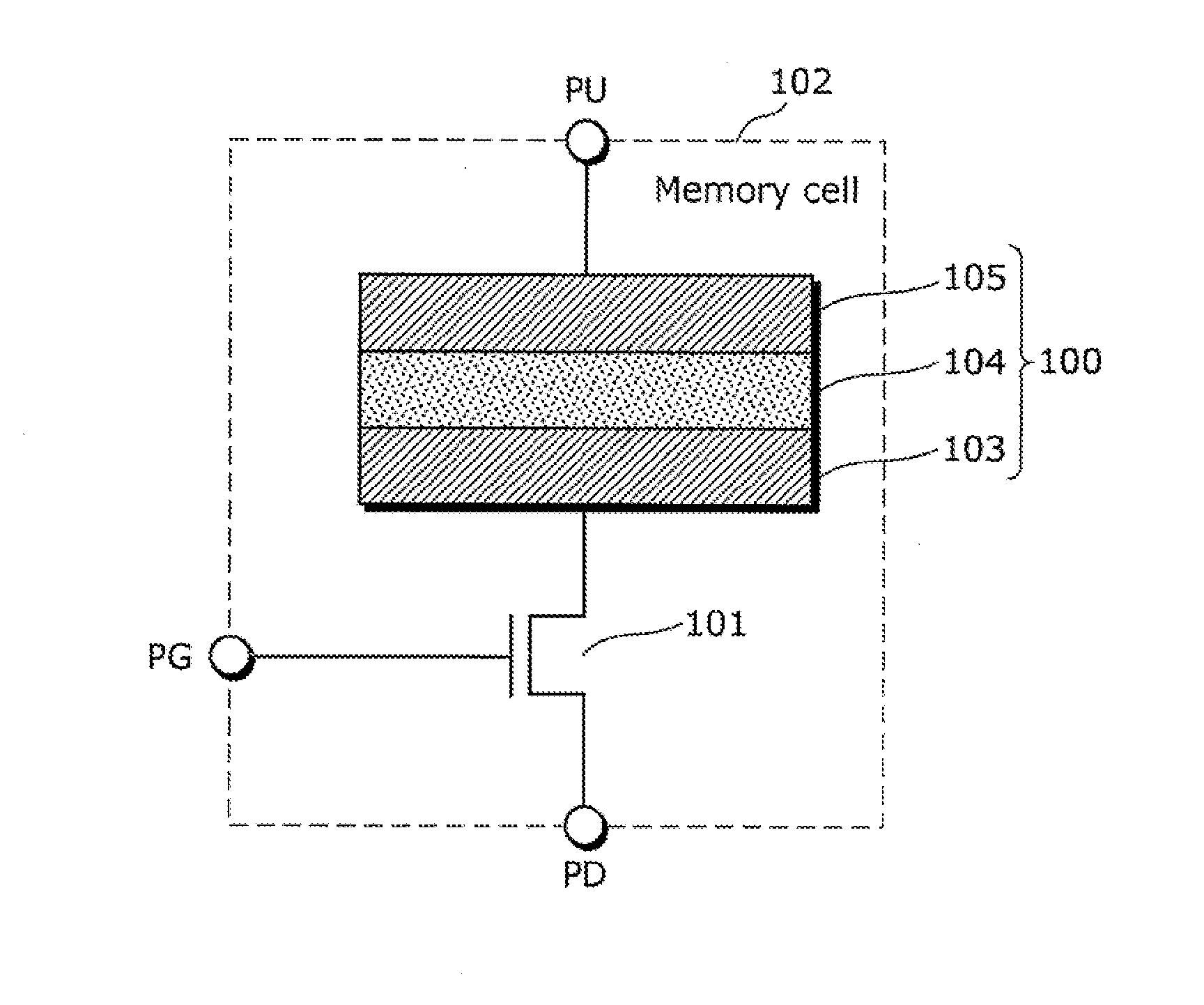
[0080]Next, a 1T1R variable resistance nonvolatile storage device (hereinafter simply referred to as nonvolatile storage device) using the aforementioned variable resistance element will be described as Embodiment 1 in the present invention for reducing variations in resistance value of a variable resistance element in the low resistance state.
[0081]FIG. 7 is a block diagram illustrating a configuration of a nonvolatile storage device according to Embodiment 1 in the present invention.
[0082]As illustrated in FIG. 7, a nonvolatile storage device 200 according to Embodiment 1 includes a memory body 201 on a semiconductor substrate. The memory body 201 includes a memory cell array 202; a column selection circuit 203; a read circuit 204 which detects an amount of a current flowing through a selected bit line and determines whether stored data indicates “1” or “0”; a data signal input and output circuit 205 which performs input and output processes on a data signal; and a write circuit 2...
embodiment 2
[0142]Next, a nonvolatile storage device according to Embodiment 2 will be described.
[0143]FIG. 12 is a block diagram illustrating a configuration of a nonvolatile storage device 200a according to Embodiment 2 in the present invention. The nonvolatile storage device 200a is different from the nonvolatile storage device 200 according to Embodiment 1 by including two reference voltage generation circuits (first reference voltage generation circuit 231 and second reference voltage generation circuit 232) and a write circuit 206a including an LR write circuit 500a including three driving circuits (first driving circuit 510, second driving circuit 540, third driving circuit 550). The differences will be described hereinafter.
[0144]FIG. 13 illustrates a specific example of a circuit configuration of the write circuit 206a according to Embodiment 2 in the present invention, and a circuit diagram indicating a power source for LR writing 220, a power source for HR writing 221, the first refe...
embodiment 3
[0165]Next, a nonvolatile storage device according to Embodiment 3 will be described. The nonvolatile storage device according to Embodiment 3 basically has the same configuration as that of the nonvolatile storage device according to Embodiment 1 in FIG. 7. However, the detailed configuration of a write circuit according to Embodiment 3 is different from that according to Embodiment 1. The differences will be described hereinafter.
[0166]FIG. 15 illustrates a specific example of a circuit configuration of a write circuit 206b according to Embodiment 3 in the present invention, and a circuit diagram indicating a power source for LR writing 220, a power source for HR writing 221, and the connection relationship between these power sources. As illustrated in FIG. 15, the write circuit 206b according to Embodiment 3 includes: an LR write circuit 500b that applies a voltage and a current to each of variable resistance elements R00, R01, . . . for changing a state thereof from a high resi...
PUM
 Abstract
Description
Claims
Application Information
 - Generate Ideas
- Intellectual Property
- Life Sciences
- Materials
- Tech Scout
- Unparalleled Data Quality
- Higher Quality Content
- 60% Fewer Hallucinations
Browse by: Latest US Patents, China's latest patents, Technical Efficacy Thesaurus, Application Domain, Technology Topic, Popular Technical Reports.
© 2025 PatSnap. All rights reserved.Legal|Privacy policy|Modern Slavery Act Transparency Statement|Sitemap|About US| Contact US: help@patsnap.com