Image reading device and image reading method

a reading device and reading method technology, applied in the field of image reading devices and image reading methods, can solve the problems of deterioration of display performance, difficult to improve a reading speed, thinner and lighter scanners, etc., and achieve the effect of improving the operability of the device and improving the reading speed

Inactive Publication Date: 2005-12-08
SHARP KK
View PDF4 Cites 46 Cited by
  • Summary
  • Abstract
  • Description
  • Claims
  • Application Information

AI Technical Summary

Benefits of technology

[0061] In this case, it is not necessary to provide a period for carrying out the fourth step, so that it is possible to shorten a period from the third step to the first step of the next cycle.
[0062] Thus, when images are sequentially read, it is possible to improve the reading speed, and it is also possible to improve the operability of the device.

Problems solved by technology

However, since a scanner having such linear sensor includes a mechanical scanning system for reading the two-dimensional image, there is limit in making the scanner thinner and lighter, so that there arises such a problem that it is difficult to improve a reading speed.
For example, in case of using the TFT as a switching element (address element) of the display device, when Vth of the TFT shifts while being used for an extended period of time, there arises such a problem that a display performance is deteriorated.
While, in case of using the TFT as a switching element (address element) of the X ray imaging device, the shift of Vth of the TFT makes a dynamic range of a detection signal smaller, so that there arises such a problem that detection of a feeble signal is unstable.
Such shifting phenomenon of Vth of the TFT is regarded as a troublesome problem caused in the case where the TFT is used as the switching element of the display device or the X ray imaging device and the device is used for an extended period of time.
Incidentally, the present inventors found that a similar problem occurs not only in the case of using the TFT as the switching element (address element) as described above but also a case of using the TFT as a photodetecting element (photodetecting TFT).
Thus, there arises the following problem.
However, when the resistance value of the TFT varies in a short time as described above, there arises such a problem that it is impossible to perform proper image correction on the basis of the correction data obtained in the first calibration operation.
Further, when influences exerted by the short-time variations of the TFT are accumulated, this causes such large variation that it is possible to restore the data, so that long-time reliability may be lost.

Method used


Image

  • Image reading device and image reading method
  • Image reading device and image reading method
  • Image reading device and image reading method

Examples


embodiment 1

[0109] One embodiment of the present invention is described below.

[0110] Note that, the present embodiment describes an example where an image reading device of the present invention is applied to a two-dimensional image sensor.

[0111] First, a photodetecting TFT (photosensor) used in the two-dimensional image sensor is described, and next, the two-dimensional image sensor will be described.

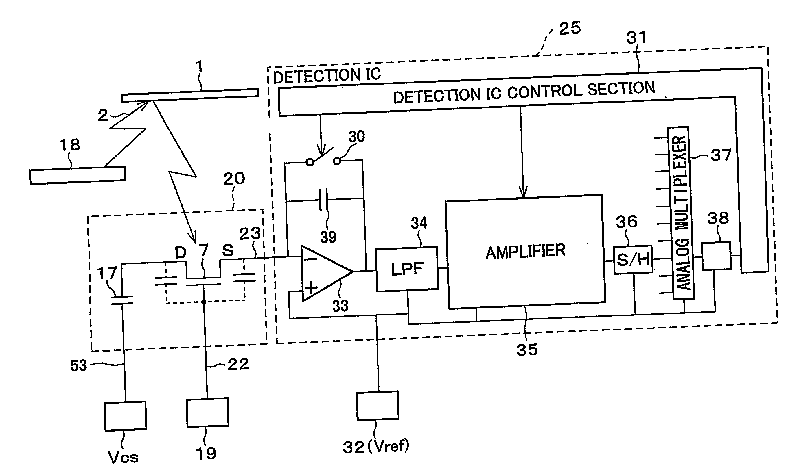
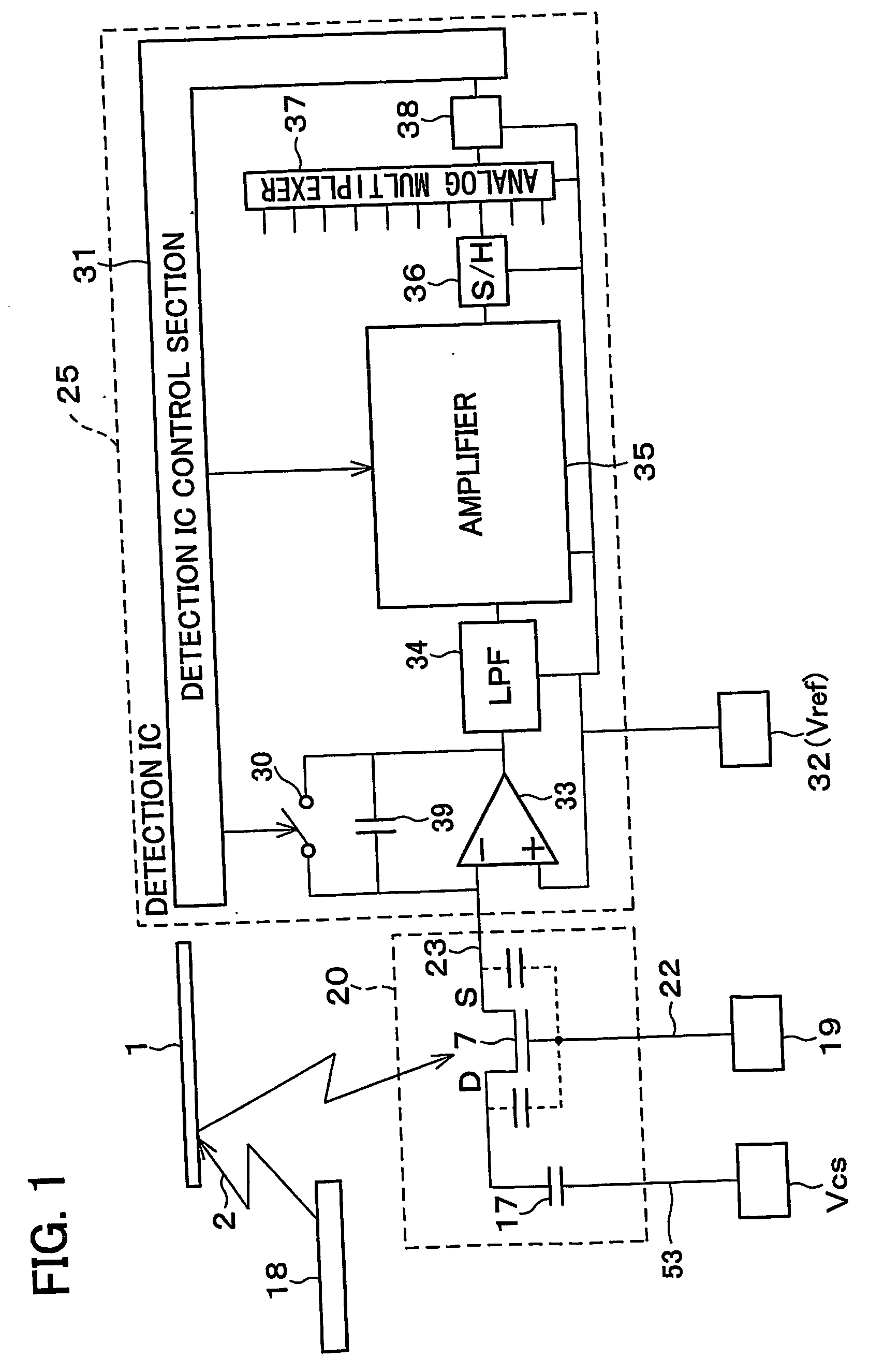
[0112] The photosensor is basically an inversely staggered thin film transistor (TFT) (as long as an upper gate electrode is made of light-transmission material, the photosensor may be the inversely staggered thin film transistor). That is, as shown in FIG. 3, the photodetecting TFT 7 is arranged so that: a bottom gate electrode 11 made of alminium (Al), tantalum (Ta), and the like is formed on an insulating substrate (transparent substrate) 9 made of glass and the like, and a gate insulating film (protection film) 13 made of silicon nitride (SiN) is formed so as to cover the bottom gate electr...

embodiment 2

[0196] Another embodiment of the present invention is described as follows. Note that, as in Embodiment 1, also the present embodiment will explain an example of the two-dimensional image sensor which functions as an image reading device.

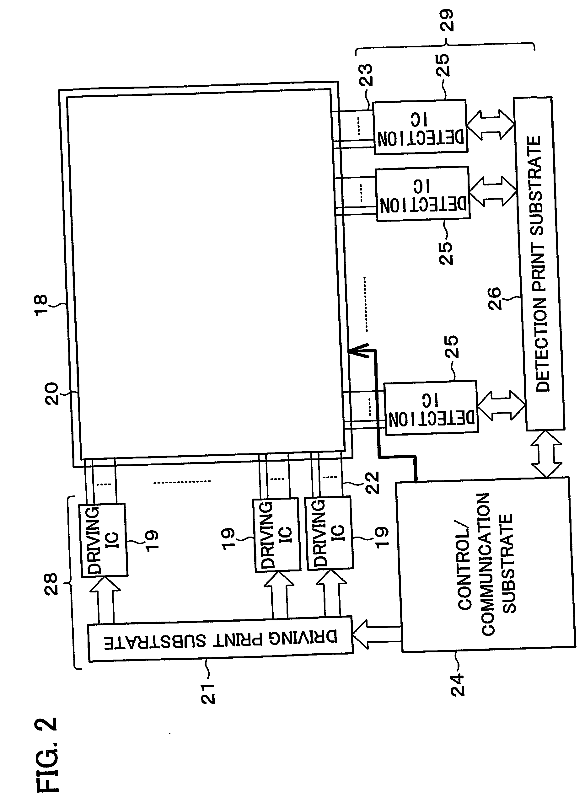
[0197] The two-dimensional image sensor according to the present embodiment includes a sensor substrate 40 shown in FIG. 21.

[0198] As shown in FIG. 21, the sensor substrate 40 includes (i) gate lines 22 each of which is extended from a driving circuit 51 as an electric wiring and (ii) data lines 23 each of which is extended from a reading circuit 52 as an electric wiring, and the gate lines 22 and the data lines 23 are disposed in an X-Y matrix manner (lattice manner), and each lattice sections each pixel. Each pixel includes: a thin film transistor (referred to as switching TFT) 41; a thin film transistor for light detection which functions as a phototransistor (referred to as photodetecting TFT) 42; and a pixel capacitor 43 which functions as an...


PUM


Abstract

The image reading device of the present invention includes (i) a sensor substrate which functions as a photoelectric transfer element having a photodetecting TFT and a pixel capacitor and (ii) a driving IC for applying a voltage to a gate electrode of the photodetecting TFT so as to drive the photodetecting TFT into an ON state or an OFF state. The driving IC applies a voltage, whose polarity is opposite to average polarity of a voltage making the photodetecting TFT in the OFF state, to the gate electrode of the photodetecting TFT in an arbitrary period. Thus, it is possible to provide the image reading device which can suppress variation of a photodetecting TFT property (resistance value) which is observed in a short time.

Description

TECHNICAL FIELD [0001] The present invention relates to an image reading device and an image reading method in which a thin film transistor having a photo response property is used as a photodetecting element. BACKGROUND ART [0002] There has been widely used a flat bed scanner, which can read a two-dimensional image by causing a linear sensor (CCD linear sensor and the like) whose pixels are disposed in a line manner (X direction) to perform line scanning (Y direction), as a contact-type image reading device for reading a document or a photograph. [0003] However, since a scanner having such linear sensor includes a mechanical scanning system for reading the two-dimensional image, there is limit in making the scanner thinner and lighter, so that there arises such a problem that it is difficult to improve a reading speed. [0004] Then, there is developed an active-matrix-type two-dimensional image sensor (image reading device), in which photodetecting elements (photodiode, phototransis...

Claims


Application Information

Patent Timeline
Patent Type & Authority Applications(United States)
IPC IPC(8): H01L27/146H01L27/14H04N1/028H04N1/031H04N1/04H04N5/335H04N5/369H04N5/376H04N5/378
CPCH01L27/14676H04N1/0318
Inventor IZUMI, YOSHIHIROUEHARA, KAZUHIROODA, TOMOHIKOTERANUMA, OSAMU
Owner SHARP KK
Why Eureka
Try Eureka