

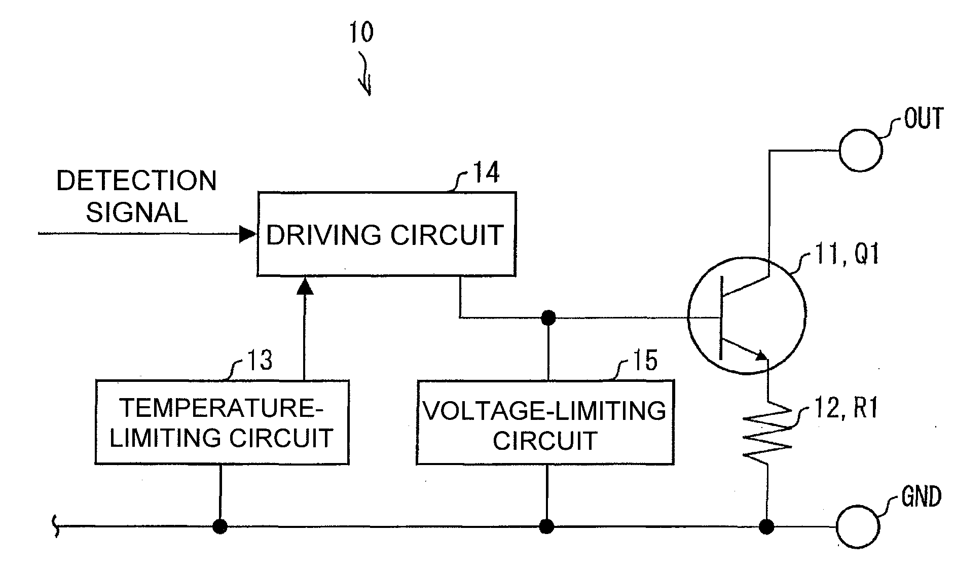
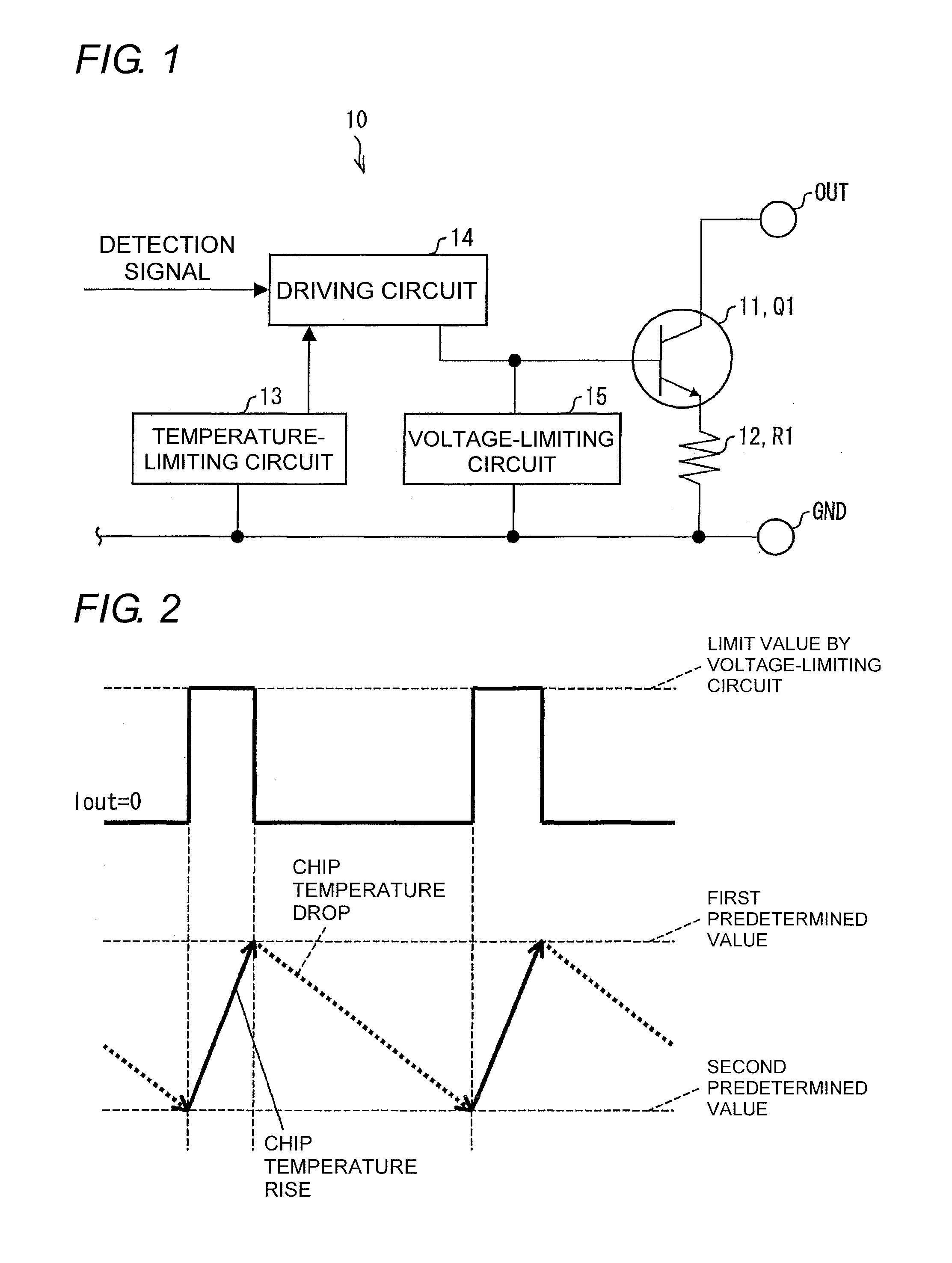
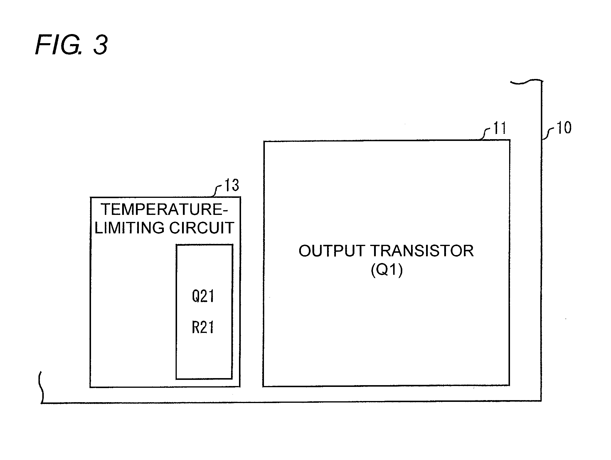
Sensor output IC and sensor device
a sensor and output technology, applied in the field of sensor output ic, can solve the problems of increasing the production cost of the sensor device, the limitation of the production process of the sensor output ic b>121/b> to an expensive one, and the troublesome short-circuit protection circuit of the conventional short-circuit protection circuit in further achieving the miniaturization and low cost of the sensor, so as to achieve advantageously reduce the production cost and circuit scale.
- Summary
- Abstract
- Description
- Claims
- Application Information
AI Technical Summary
Benefits of technology
Problems solved by technology
Method used
Image

Examples
first example
[0048]FIG. 4 illustrates a first example of a circuit of the sensor output IC 10 of FIG. 1. First an example of the driving circuit 14 in the sensor output IC 10 will be described. As illustrated in FIG. 4, the driving circuit 14 includes a constant current source CC11, NPN transistors Q11 and Q12, and a resistor R11.
[0049]In the transistor Q11, the collector terminal is connected to a power supplying terminal VCC, the detection signal is inputted to the base terminal from the sensor 120, and the emitter terminal is connected to the base terminal of the output transistor 11 through the resistor R11. In the transistor Q12, the collector terminal is connected to the constant current source CC11 and the base terminal of the transistor Q11, the base terminal is connected to the emitter terminal of the transistor Q11, and the emitter terminal is connected to the base terminal of the output transistor 11.
[0050]When the current is supplied from the constant current source CC11 to the trans...
second example
[0067]FIG. 5 illustrates a second example of a circuit of the sensor output IC 10 of FIG. 1. The second example illustrated in FIG. 5 differs from the first example illustrated in FIG. 4 only in the configuration of the voltage-limiting circuit 15, and other configurations of the second example are identical to those of the first example.
[0068]In the first example, the current Iout passed through the output transistor 11 is detected by the base potential VB at the output transistor 11 based on Equation 1. On the other hand, in the second example, the current Iout passed through the output transistor 11 is detected by the potential (emitter potential) VE at the emitter terminal of the output transistor 11. In other words, in the second example, the current Iout passed from the output transistor 11 to the resistor 12 is detected by the voltage VE at the resistor 12. Components having similar functions are designated by the same reference numerals, and the description thereof will not ...
PUM
 Abstract
Description
Claims
Application Information