Semiconductor memory device

Active Publication Date: 2019-08-01
WINBOND ELECTRONICS CORP
View PDF24 Cites 0 Cited by
  • Summary
  • Abstract
  • Description
  • Claims
  • Application Information

AI Technical Summary

Benefits of technology

[0015]According to the disclosure, constant currents flow through the resistor connected between the first node and the second node with use of the first current source and the second current source connected to the first current path and the second current path, so as to generate the voltage from the second node. Therefore, unlike the related art, the desired

Problems solved by technology

Therefore, the circuit scale becomes large.
However, in the current circuit, it is difficult to generate the driving voltage in consideration of the substrate bias effect at the same time as the high voltage programming voltage and erasing voltage, and regardless of the value of the boosted v

Method used


Image

  • Semiconductor memory device
  • Semiconductor memory device
  • Semiconductor memory device

Examples


Embodiment Construction

[0022]Hereinafter, embodiments of the disclosure will be described in detail with reference to the drawings. In an embodiment, a semiconductor memory device according to the disclosure is a NAND type flash memory, but it is only an example, and it may be a semiconductor memory having another configuration.

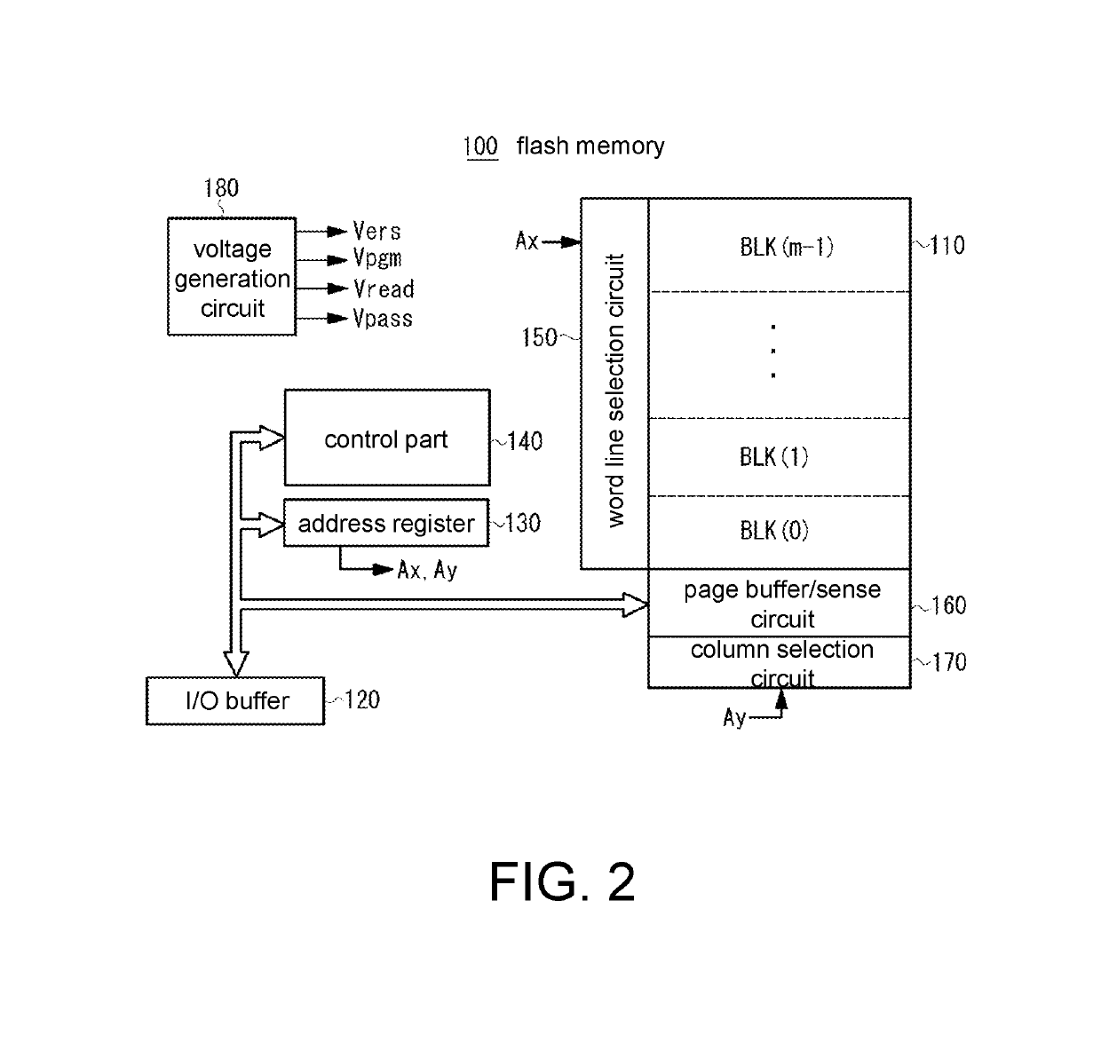
[0023]FIG. 2 shows the configuration of a flash memory according to an embodiment of the disclosure. As shown in the figure, the flash memory 100 includes a memory array 110 having a plurality of memory cells arranged in rows and columns; an I / O buffer 120 connected to an external input / output terminal I / O and holding input / output data; an address register 130 receiving address data from the I / O buffer 120; a control part 140 receiving command data from the I / O buffer 120 or an external control signal and controlling each part; a word line selection circuit 150 receiving row address information Ax from the address register 130 and selecting a block and selecting a word line or the ...


PUM


Abstract

A voltage generation circuit, having a circuit scale significantly reduced as compared with the related art, is provided. The voltage generation circuit of the disclosure includes a charge pump outputting a boosted voltage to an output node, a resistor connected between the output node and another output node, and a current source circuit having first and second current paths connected in parallel between the another output node and a reference potential. The first current path includes a resistor and a first DAC. The first DAC generates a first constant current corresponding to a voltage generation code. The second current path includes a second DAC. The second DAC generates a second constant current corresponding to a code obtained by inverting the voltage generation code. Thereby, a driving voltage obtained by lowering the boosted voltage is generated at the other output node.

Description

CROSS-REFERENCE TO RELATED APPLICATION[0001]This application claims the priority benefit of Japan application serial no. 2018-013282, filed on Jan. 30, 2018. The entirety of the above-mentioned patent application is hereby incorporated by reference herein and made a part of this specification.BACKGROUNDTechnical Field[0002]The disclosure relates to a semiconductor memory device, such as a flash memory, and more particularly relates to a voltage generation circuit using a booster circuit.Description of Related Art[0003]In a NAND type or NOR type flash memory or the like, a high voltage is required for data reading, programming, and erasing operations. Normally, in the flash memory, a power source voltage supplied from the outside is boosted by a charge pump, and the programming, erasing, and the like are performed using the boosted voltage. In Japanese Laid-open Patent Application No. 2002-197882, a technology has been started for self-boosting a signal for reducing the charge pump a...

Claims


Application Information

Patent Timeline
IPC IPC(8): G11C16/30G11C16/14H02M3/07G11C16/08
CPCG11C16/30G11C16/14H02M3/07G11C16/08H03K5/2472G11C16/0483G11C16/225G11C16/3404G11C5/147
Inventor MURAKAMI, HIROKI
Owner WINBOND ELECTRONICS CORP
Why Eureka
Try Eureka