Drive device and method for controlling drive device
Active Publication Date: 2021-03-11
SHINDENGEN ELECTRIC MFG CO LTD
View PDF0 Cites 0 Cited by
Summary
Abstract
Description
Claims
Application Information
AI Technical Summary
This helps you quickly interpret patents by identifying the three key elements:
Problems solved by technology
Method used
Benefits of technology
Benefits of technology
The present invention is a drive device that includes a power supply terminal, a grounding terminal, and two transistors. The device also includes a first DC power supply, a first bootstrap circuit, a first stabilizing capacitor, a first gate driver circuit, a second gate driver circuit, and a first charge pump circuit. This results in a reduction in circuit size and the use of a negative power supply voltage to improve efficiency. The device is designed to suppress malfunctions in a short dead time while reducing circuit size.
Problems solved by technology
However, this conventional drive device cannot generate a negative power supply, so it is necessary to increase the dead time (FIG. 5).
As described above, the conventional drive device has a problem that the malfunction of the transistor cannot be suppressed in a short dead time while reducing the circuit scale.
Method used
Image
Click on the blue label to locate the original text in one second.
Reading with bidirectional positioning of images and text.
Examples
first embodiment
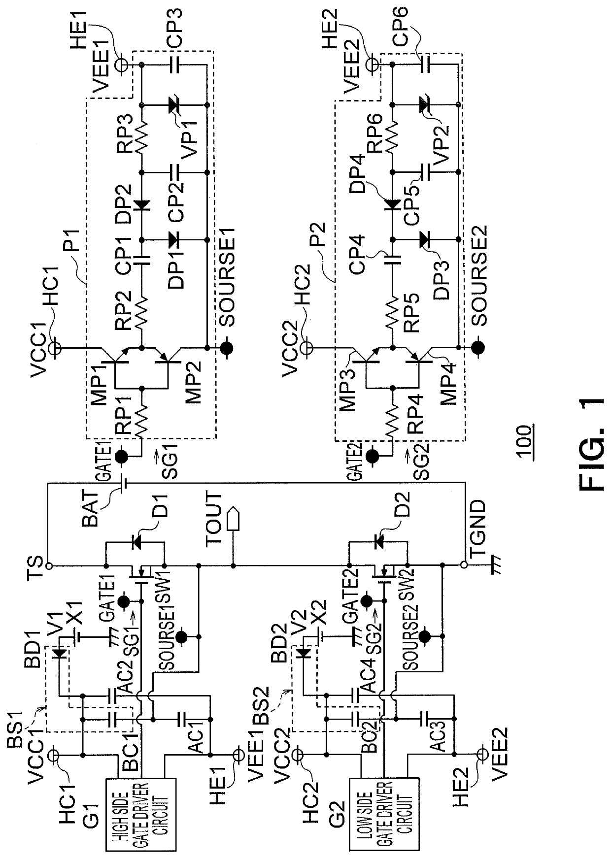
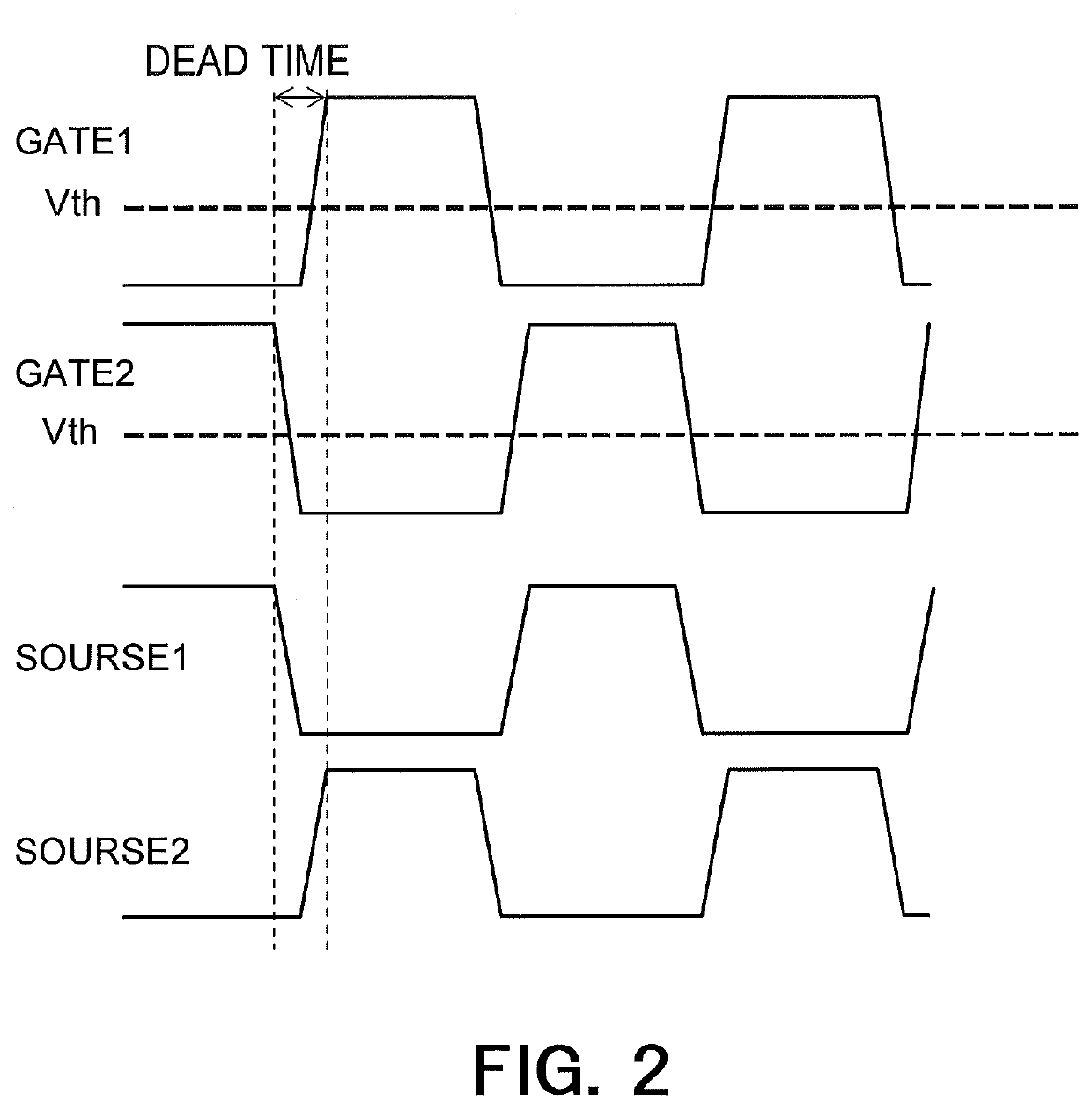
[0075]FIG. 1 is a diagram illustrating an example of the configuration of the drive device 100 according to the first embodiment. FIG. 2 is a diagram showing an example of operation waveforms of drive device 100 shown in FIG. 1.
[0076]As shown in FIG. 1, the drive device 100 outputs a predetermined voltage from the output terminal TOUT, by controlling the first transistor SW1 and the second transistor SW2 to turn on / off in a complementary manner.
[0077]Here, for example, as shown in FIG. 1, the drive device 100 includes a power supply terminal TS, a ground terminal TGND, a first transistor SW1, a second transistor SW2, a first body diode D1, a second body diode D2, a first DC (Direct Current) power supply X1, and a second DC power supply X2, a first bootstrap circuit BS1, a first stabilizing capacitor AC1, a second stabilizing capacitor AC2, a second bootstrap circuit BS2, a third stabilizing capacitor AC3, a fourth stabilizing capacitor AC4, a first gate driver circuit G1, a second g...
second embodiment
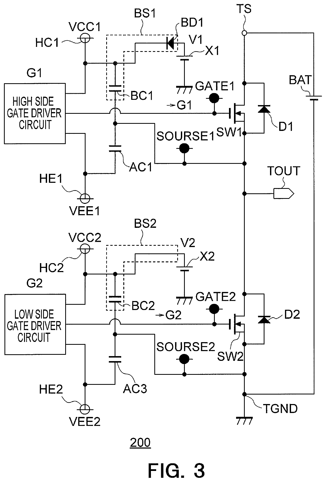
[0154]As described above, in the driving apparatus 100 according to the first embodiment, if necessary, any or all of the second stabilizing capacitor AC2, the second bootstrap diode BD2 of the second bootstrap circuit BS2, and the fourth stabilizing capacitors AC4 may be omitted.
[0155]Therefore, in the second embodiment, another configuration example of the drive device in which the above configuration is omitted will be described.
[0156]Here, FIG. 3 is a diagram illustrating an example of the configuration of the drive device 200 according to the second embodiment. In FIG. 3, the same reference numerals as those in FIG. 1 indicate the same configurations as those in the first embodiment.
[0157]The drive device 200 according to the second embodiment has, for example, as shown in FIG. 3, a configuration in which the second stabilizing capacitor AC2, the fourth stabilizing capacitor AC4 and the second bootstrap diode BD2 of the second bootstrap circuit BS2 are omitted, compared with th...
PUM
Abstract
A drive device includes a first gate driver circuit that controls operations of the first transistor by outputting a first control signal to a control terminal of the first transistor; a second gate driver circuit that controls operations of the second transistor so that the first transistor and the second transistor are turned on / off in a complementary manner, by outputting a second control signal to the control terminal of the second transistor; and a first charge pump circuit that applies the first negative power supply voltage to the first negative power supply wiring, by generating the first negative power supply voltage having a polarity opposite to that of the first positive power supply voltage with reference to a potential of the output terminal, based on the first control signal.
Description
TECHNICAL FIELD[0001]The present invention relates to a drive device and a method for controlling a drive device.BACKGROUND ART[0002]Conventionally, there is a driving device that controls the high side transistor and the low side transistor to be turned on / off in a complementary manner (see, for example, JP A 2016-67194).[0003]In this conventional drive device, when the above-mentioned two transistors (n-channel FET) are turned on / off and the high-side transistor turns on, the source potential of the high side transistor and the drain potential of the low side transistor rise, and dv / dt rises.[0004]At this time, the gate potential of the low-side transistor rises due to the current flowing through the drain-gate parasitic capacitance of the low side transistor and the gate resistance.[0005]Then, when the gate potential exceeds the threshold voltage Vth of the low side transistor, the low side transistor is turned on, and the high side transistor and the low side transistor are arm-...
Claims
Application Information
Patent Timeline
Application Date:The date an application was filed.
Publication Date:The date a patent or application was officially published.
First Publication Date:The earliest publication date of a patent with the same application number.
Issue Date:Publication date of the patent grant document.
PCT Entry Date:The Entry date of PCT National Phase.
Estimated Expiry Date:The statutory expiry date of a patent right according to the Patent Law, and it is the longest term of protection that the patent right can achieve without the termination of the patent right due to other reasons(Term extension factor has been taken into account ).
Invalid Date:Actual expiry date is based on effective date or publication date of legal transaction data of invalid patent.

