Soi radio frequency switch with enhanced signal fidelity and electrical isolation

a radio frequency switch and enhanced signal technology, applied in the field of semiconductor structures, can solve problems such as reducing the effectiveness of rf switches

Active Publication Date: 2011-09-15
TAIWAN SEMICON MFG CO LTD
View PDF17 Cites 15 Cited by
  • Summary
  • Abstract
  • Description
  • Claims
  • Application Information

AI Technical Summary

Benefits of technology

In the present invention, a doped contact region having an opposite conductivity type as a bottom semiconductor layer is formed underneath a buried insulator layer in a bottom semiconductor layer of a semiconductor-on-insulator (SOI) substrate. At least one conductive via structure is formed, which extends from an interconnect-level metal line through a middle-of-line (MOL) dielectric layer, a shallow trench isolation structure in a top semiconductor layer, and a buried insulator layer and to the doped contact region. During operation, the doped contact region is biased at a voltage that is at, or close to, a peak voltage in the RF switch to prevent formation of an inversion layer within the induced charge layer. The charges in the inversion layer are drained through the doped contact region and the at least one conductive via structure. Rapid discharge of the minority charge carriers reduces harmonic generation and signal distortion in the RF switch.

Problems solved by technology

The spurious capacitive coupling between the induced charge layer in the bottom semiconductor layer and the other semiconductor devices provides a secondary capacitive coupling, which is a parasitic coupling that reduces the effectiveness of the RF switch.

Method used


Image

  • Soi radio frequency switch with enhanced signal fidelity and electrical isolation
  • Soi radio frequency switch with enhanced signal fidelity and electrical isolation
  • Soi radio frequency switch with enhanced signal fidelity and electrical isolation

Examples


first embodiment

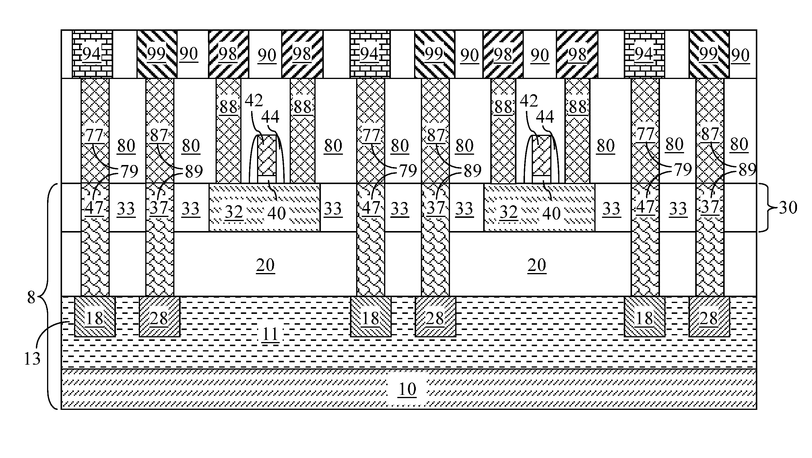
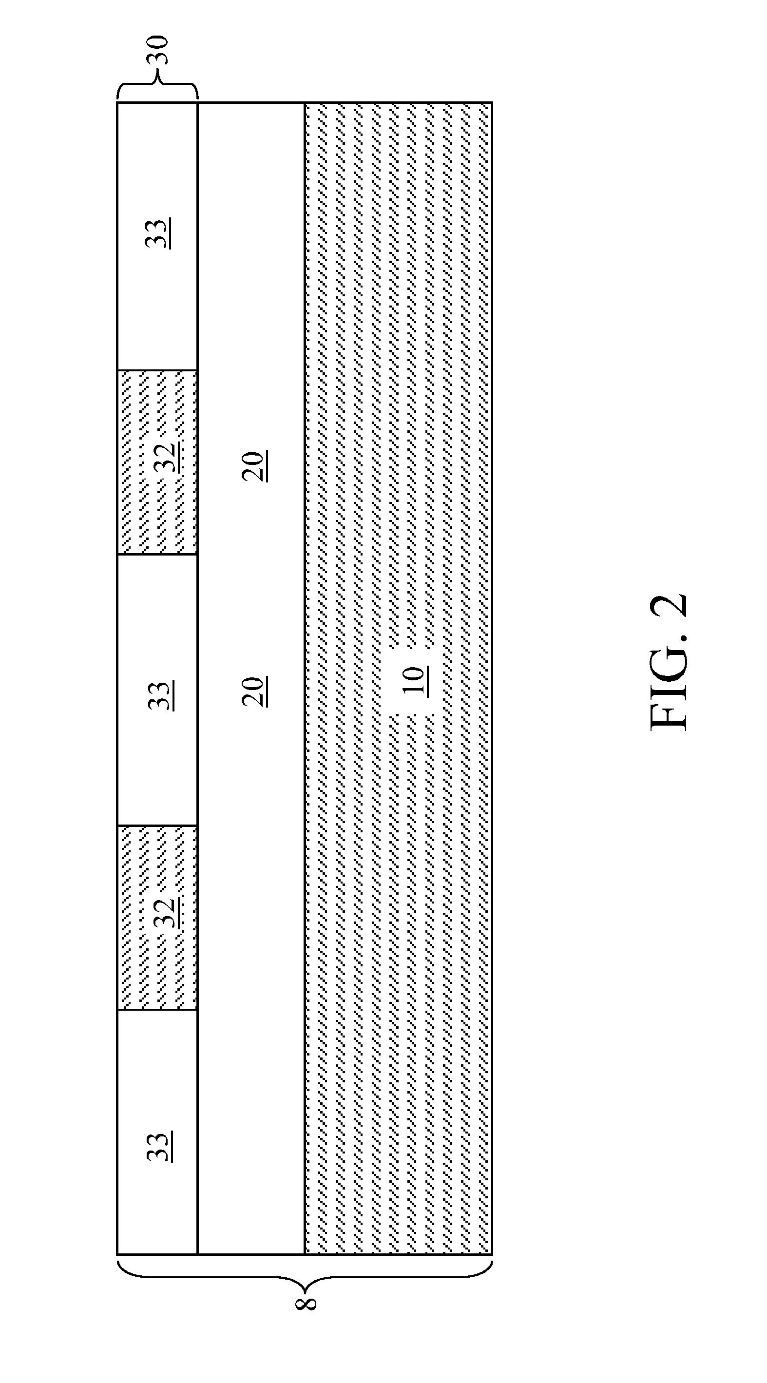
Referring to FIG. 2, a first exemplary semiconductor structure according to the present invention comprises a semiconductor substrate 8. The semiconductor substrate 8 is a semiconductor-on-insulator (SOI) substrate that includes a bottom semiconductor layer 10, a buried insulator layer 20, and a top semiconductor layer 30. The top semiconductor layer 30 includes at least one top semiconductor portion 32 and a shallow trench isolation structure 33. At least one pad dielectric layer (not shown) comprising at least one dielectric material, such as silicon nitride and / or silicon nitride, may be provided on a top surface of the top semiconductor layer 30 to facilitate formation of lower conductive vias by planarization in subsequent processing steps.

Each of the bottom semiconductor layer 10 and the at least one top semiconductor portion 32 comprises a semiconductor material such as silicon, a silicon germanium alloy region, silicon, germanium, a silicon-germanium alloy region, a silicon ...

second embodiment

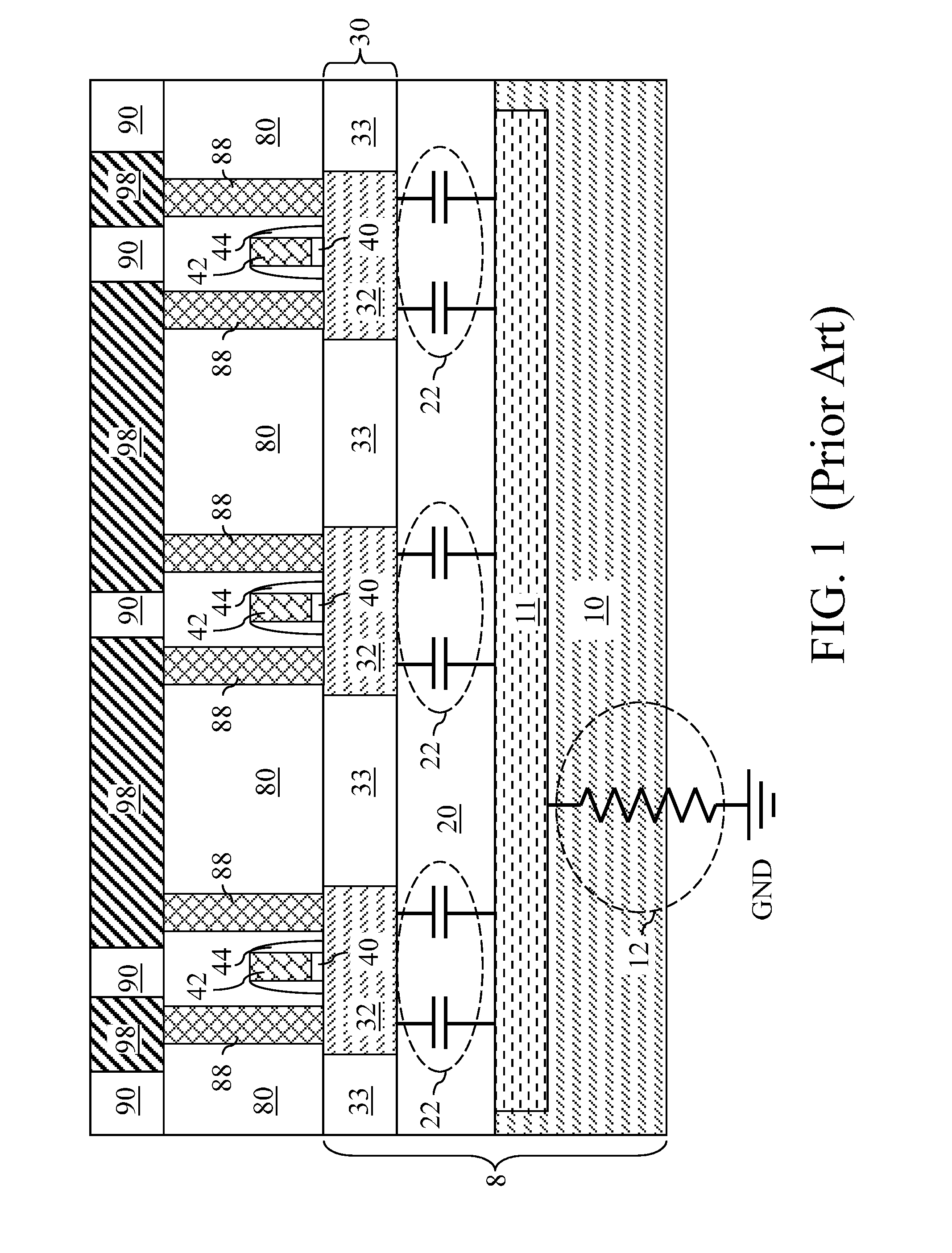
At such high frequencies, capacitive coupling between the at least one field effect transistor and the bottom semiconductor layer 10 may become significant since the capacitive coupling increases linearly with frequency. The radio frequency signal in the at least one field effect transistor causes formation of an induced charge layer 11 in an upper portion of the bottom semiconductor layer 10. In the second embodiment, the induced charge layer 11 is formed directly underneath the buried insulator layer 11, and includes positive charges or negative charges depending on the phase of the radio frequency signal in the at least one field effect transistor.

Referring to FIG. 24, when the phase of the radio frequency signal is such that majority charge carriers are repelled from an upper portion of the bottom semiconductor layer 10, the induced charge layer 11 comprises a depletion region. Further, a strong RF signal attracts minority charge carriers directly underneath the bottom surface o...


PUM


Abstract

A doped contact region having an opposite conductivity type as a bottom semiconductor layer is provided underneath a buried insulator layer in a bottom semiconductor layer. At least one conductive via structure extends from an interconnect-level metal line through a middle-of-line (MOL) dielectric layer, a shallow trench isolation structure in a top semiconductor layer, and a buried insulator layer and to the doped contact region. The doped contact region is biased at a voltage that is at or close to a peak voltage in the RF switch that removes minority charge carriers within the induced charge layer. The minority charge carriers are drained through the doped contact region and the at least one conductive via structure. Rapid discharge of mobile electrical charges in the induce charge layer reduces harmonic generation and signal distortion in the RF switch. A design structure for the semiconductor structure is also provided.

Description

FIELD OF THE INVENTIONThe present invention relates to semiconductor structures, and particularly to a semiconductor structure including a radio frequency switch on a semiconductor-on-insulator (SOI) substrate, methods of manufacturing the same, and methods of operating the same.BACKGROUNDSemiconductor devices such as field effect transistors are employed as a switching device for radio frequency (RF) signals in analog and RF applications. Semiconductor-on-insulator (SOI) substrates are typically employed for such applications since parasitic coupling between devices through the substrate is reduced due to the low dielectric constant of a buried insulator layer. For example, the dielectric constant of silicon, which comprises the entirety of the substrate of a bulk silicon substrate, is about 11.7 in gigahertz ranges. In contrast, the dielectric constant of silicon oxide, which isolates a top semiconductor layer containing devices from a handle substrate, is about 3.9. By providing ...

Claims


Application Information

Patent Timeline
Patent Type & Authority Applications(United States)
IPC IPC(8): H03K3/01H01L21/336G06F17/50
CPCH01L21/76224H01L27/1203H01L21/84H01L21/76251H01L21/743H01L21/02225
Inventor BOTULA, ALAN B.JOSEPH, ALVIN J.NOWAK, EDWARD J.SHI, YUNSLINKMAN, JAMES A.
Owner TAIWAN SEMICON MFG CO LTD
Why Eureka
Try Eureka