Semiconductor storage device and its cell activation method
- Summary
- Abstract
- Description
- Claims
- Application Information
AI Technical Summary
Benefits of technology
Problems solved by technology
Method used
Image


Examples
first embodiment
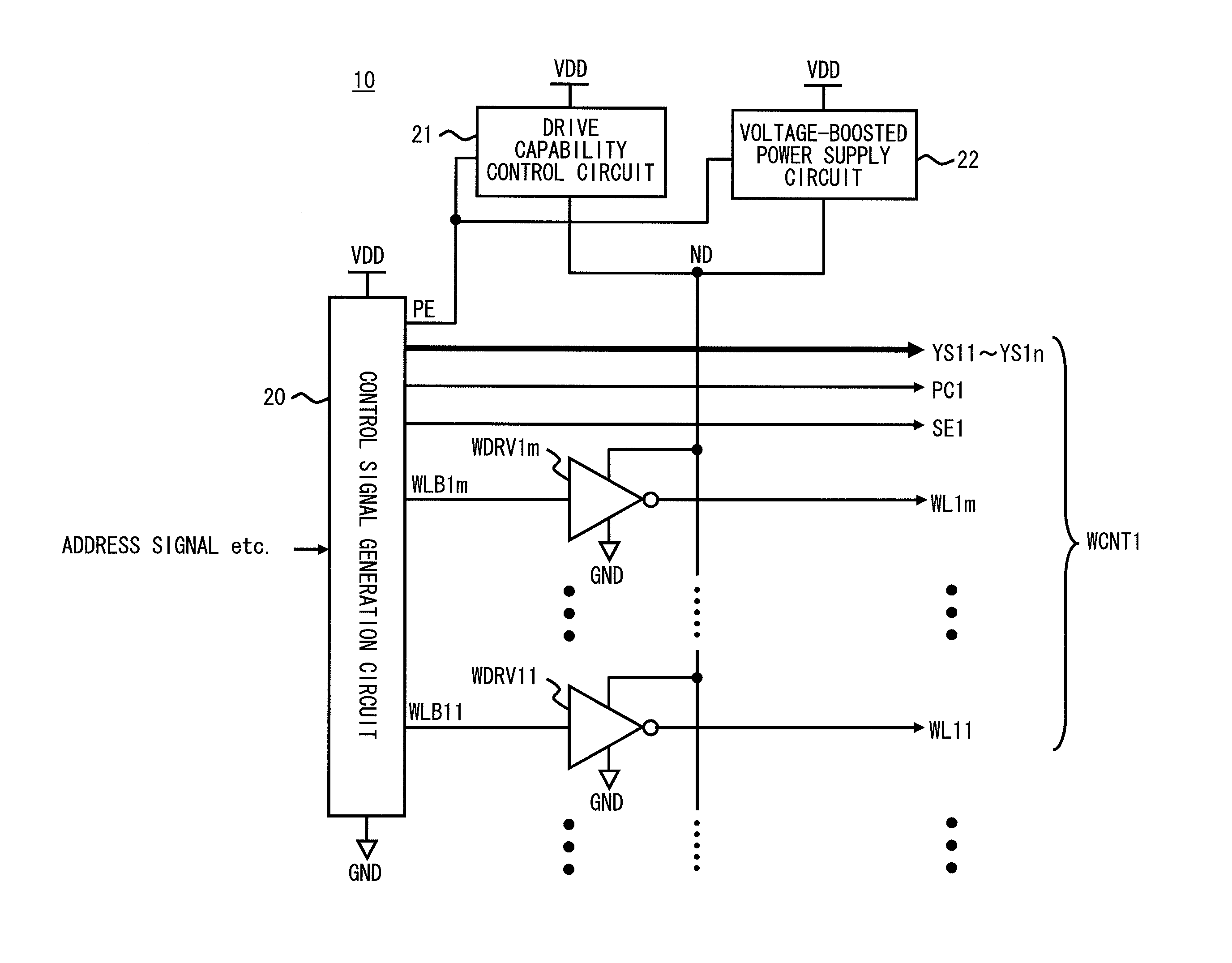
[0031]Embodiments in accordance with the present invention are explained hereinafter with reference to the drawings. Firstly, FIG. 1 shows a block diagram of a semiconductor storage device 1 in accordance with a first embodiment of the present invention. Although the following explanation is made while focusing attention on the functions of an SRAM as a semiconductor storage device, the semiconductor storage device in accordance with the present invention may be a semiconductor storage device in which an SRAM is integrally formed with other functional circuits such as a CPU. The semiconductor storage device 1 shown in FIG. 1 includes a word line control circuit 10, an I / O circuit 11 in which a sense amplifier SA and a write control circuit WA are disposed, and a plurality of SRAM circuits 12. In this embodiment, all of the word line control circuit 10, the I / O circuit 11, and the SRAM circuits 12 operate based on a first power supply potential (e.g., power supply potential supplied ...
PUM
 Abstract
Description
Claims
Application Information