
Bottom electrodes for use with metal oxide resistivity switching layers

a resistivity switching and bottom electrode technology, applied in the field of memory arrays, can solve the problem of difficult fabrication of memory devices from metal oxide rewriteable resistivity switching materials with desirable switching characteristics

Active Publication Date: 2011-09-22
SANDISK TECH LLC
View PDF49 Cites 251 Cited by
  • Summary
  • Abstract
  • Description
  • Claims
  • Application Information

AI Technical Summary

Benefits of technology

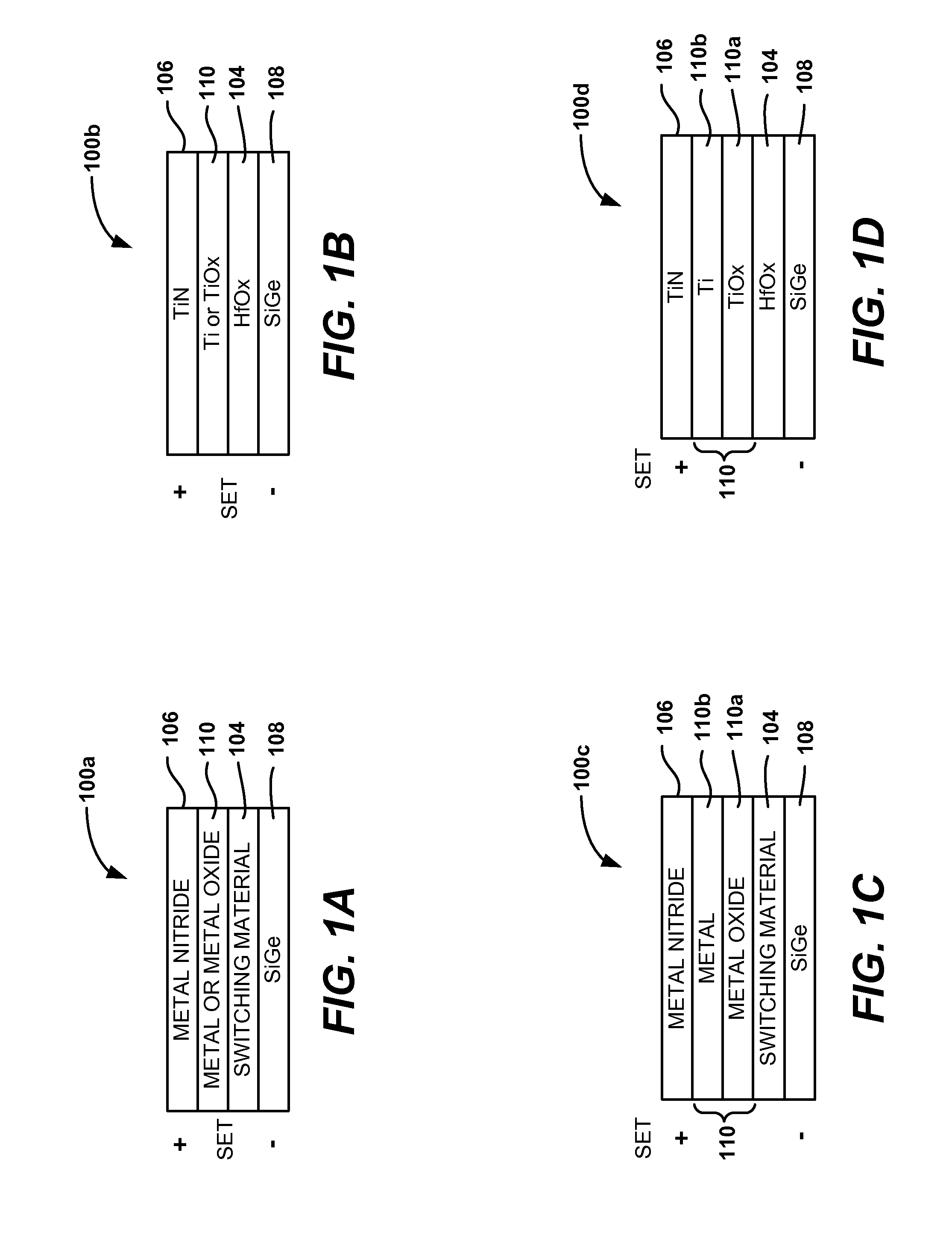
[0012]In an eighth aspect of the invention, an MIM stack is provided that includes (1) a first conductive layer comprising one or more of chromium, chromium nitride, hafnium, hafnium nitride, niobium, niobium nitride, vanadium, vanadium nitride, zirconium or zirconium nitride; (2) a resistivity-switching layer comprising a metal oxide layer formed above the first conductive layer; and (3) a second conductive layer formed above the resistivity-switching layer. A memory cell may be formed from the MIM stack.
[0013]In a ninth aspect of the

Problems solved by technology

However, fabricating memory devices from metal oxide rewriteable resistivity-switching materials with desirable switching characteristics is difficult; and improved memory devices that employ metal oxide resistivity-switching materials are desirable.

Method used


Image

  • Bottom electrodes for use with metal oxide resistivity switching layers
  • Bottom electrodes for use with metal oxide resistivity switching layers
  • Bottom electrodes for use with metal oxide resistivity switching layers

Examples


Embodiment Construction

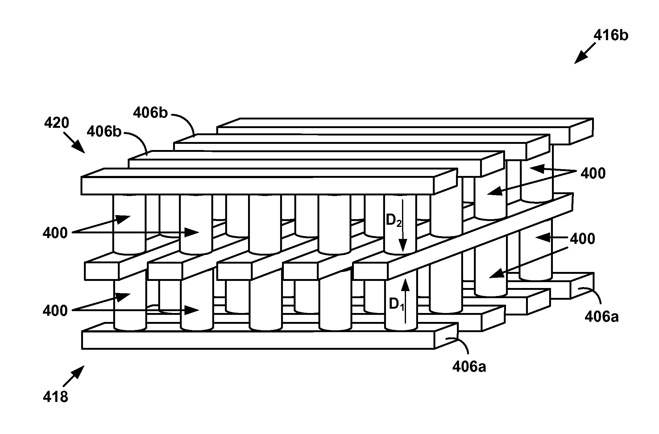
[0025]A metal-insulator-metal (MIM) stack formed from a reversible resistivity switching (RRS) material sandwiched between two metal or otherwise conducting layers may serve as a resistance-switching element for a memory cell. The two conducting layers may serve as the top and bottom electrodes of the resistance-switching element, and may be used to apply an electric field across the RRS material that changes the resistivity of the RRS material from a high value to a low value and vice versa.

[0026]In accordance with embodiments of the present invention, novel MIM stacks are provided that employ metal oxide resistivity-switching layers. Methods of forming such MIM stacks, as well as methods of employing such MIM stacks in three-dimensional (3D) memory arrays, are also provided.

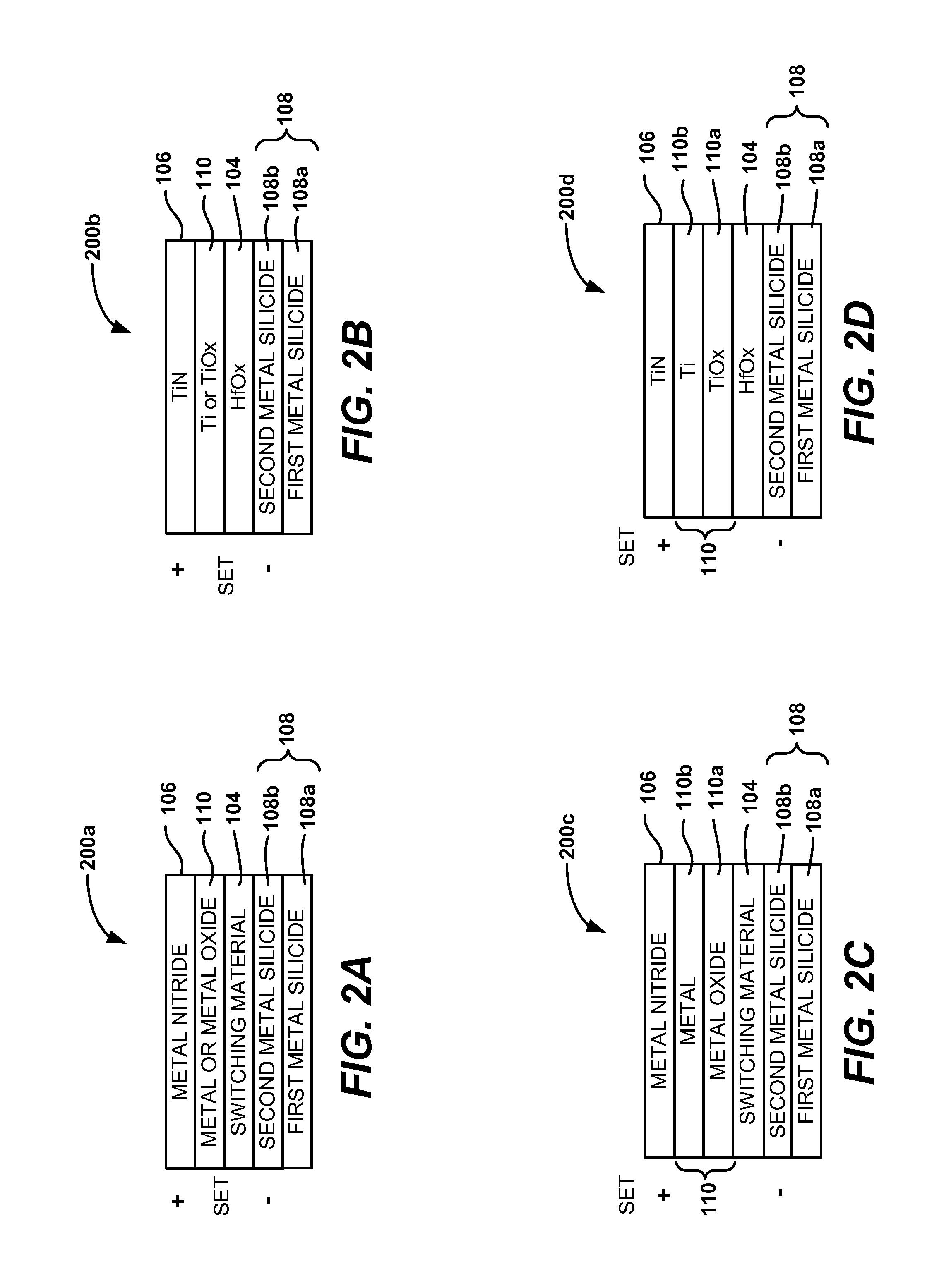
[0027]These and other embodiments of the invention are described below with reference to FIGS. 1A-5H. For example, FIGS. 1A-1D illustrate MIM stacks that employ SiGe bottom electrodes. FIGS. 2A-2H illustrate MI...


PUM


Abstract

In a first aspect, an MIM stack is provided that includes (1) a first conductive layer comprising a first metal-silicide layer and a second metal-silicide layer; (2) a resistivity-switching layer comprising a metal oxide layer formed above the first conductive layer; and (3) a second conductive layer formed above the resistivity-switching layer. A memory cell may be formed from the MIM stack. Numerous other aspects are provided.

Description

RELATED APPLICATIONS[0001]The present application claims priority to U.S. Provisional Patent Application Ser. No. 61 / 314,577, filed Mar. 16, 2010 and titled “ELECTRODES FOR USE WITH RESISTIVITY SWITCHING MATERIALS”, which is hereby incorporated by reference herein in its entirety for all purposes.FIELD OF THE INVENTION[0002]The present invention relates to memory arrays and more particularly to bottom electrodes for use with metal oxide resistivity switching layers.BACKGROUND OF THE INVENTION[0003]Reversible resistivity-switching (RRS) materials such as metal oxides may be used as storage elements in memory arrays. For example, U.S. Pat. No. 7,812,404, filed May 9, 2005 and titled “NON-VOLATILE MEMORY CELL COMPRISING A DIODE AND A RESISTANCE-SWITCHING MATERIAL”, which is hereby incorporated by reference herein in its entirety, describes a rewriteable non-volatile memory cell that includes a diode coupled in series with an RRS material such as a metal oxide or metal nitride.[0004]How...

Claims


Application Information

Patent Timeline
IPC IPC(8): H01L45/00
CPCH01L45/145H01L45/1253H01L45/1675H01L27/2481H01L45/1233H01L45/146H01L27/2409H01L45/08H10B63/20H10B63/84H10N70/24H10N70/826H10N70/841H10N70/8833H10N70/063H10B63/00H10N70/00H10N70/883
Inventor SEKAR, DEEPAK CHANDRAKREUPL, FRANZMAKALA, RAGHUVEER S.
Owner SANDISK TECH LLC
Learn More