Electroforming method

a technology of electroforming and metal-forming products, applied in the field of electroforming methods, can solve the problems of reducing the moldable shape of metal-formed products, reducing the efficiency of manufacturing, and increasing the cost of manufacturing

Active Publication Date: 2011-09-29
ORMON CORP
View PDF3 Cites 18 Cited by
  • Summary
  • Abstract
  • Description
  • Claims
  • Application Information

AI Technical Summary

Benefits of technology

[0026]According to one or more embodiments of the present invention, the growth of the metal layer is stopped, with a space left above the metal layer with a height according to the width of the recessed part. Therefore, an electric current flows from the side of the metal layer to make the thickness of the formed metal layer uniform in a growing direction, and no finish is required to be performed on the surface opposite to the mold.

Problems solved by technology

However, in the process of electrodepositing a metal on the surface of the mold, part of an electric current interrupted by the resist film flows into an electrodeposited part near the resist film to partially increase the amount of electrodeposition, resulting in a trouble of unevenness of the thickness of the metal layer.
As described above, in conventional electroforming, the surface of the metal layer (a surface opposite to a surface electrodeposited on a mold) cannot be controlled, which considerably restricts the moldable shape of a metal-formed product.
Also, in order to put the shape of the metal-formed product properly, polishing or the like has to be performed after forming, which decreases efficiency of manufacture and increases cost of manufacture.

Method used


Image

  • Electroforming method
  • Electroforming method
  • Electroforming method

Examples


first embodiment

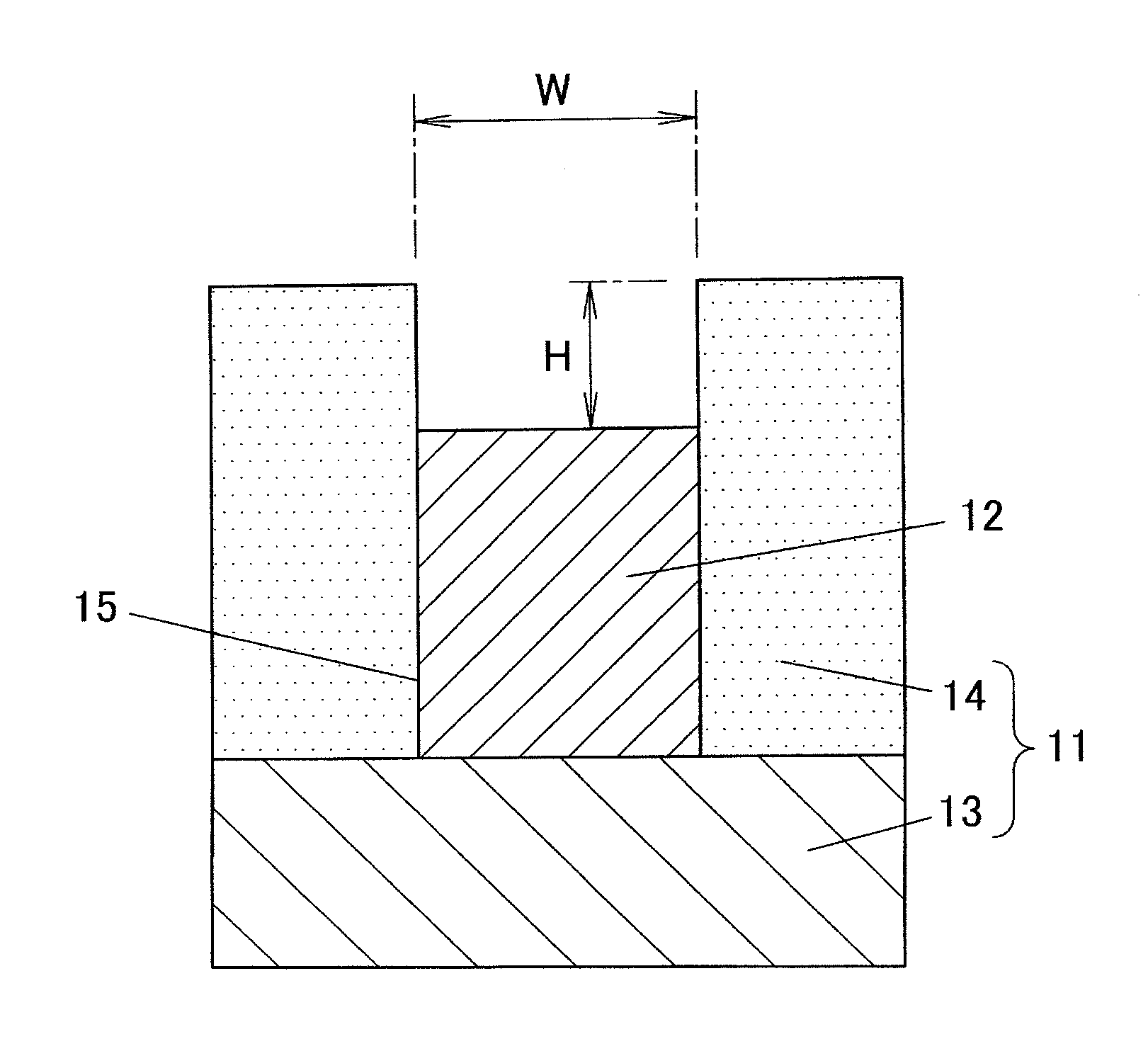
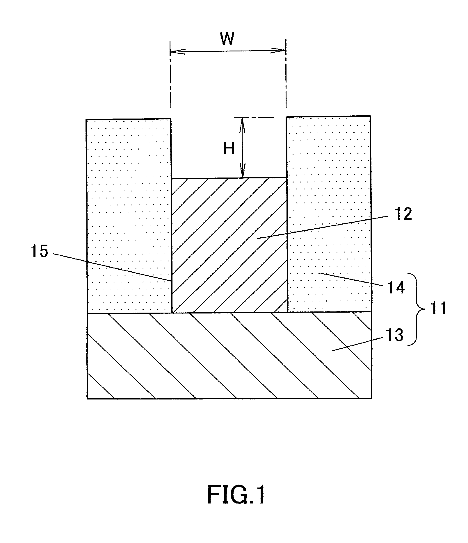
[0059]FIG. 1 is a sectional view for describing an electroforming method (hereinafter referred to electroforming) according to a first embodiment of the present invention, depicting a mold 11 and a metal-formed product 12 electroformed by using the mold 11.

[0060]The mold 11 for use in the first embodiment is produced by laminating a thick insulating layer 14 on a flat upper surface of a conductive base material 13. In the insulating layer 14, a cavity 15 (a recessed part) in a reversed shape of the metal-formed product 12 is formed. On the bottom surface of the cavity 15, no insulating layer 14 is left, and an upper surface of the conductive base material 13 is exposed from the entire bottom surface of the cavity 15. In the cavity 15 of the mold 11, the metal-formed product 12 is formed by electroforming. Note that FIG. 1 depicts a cross section of the cavity 15 in a direction (a transverse direction) orthogonal to a longitudinal direction.

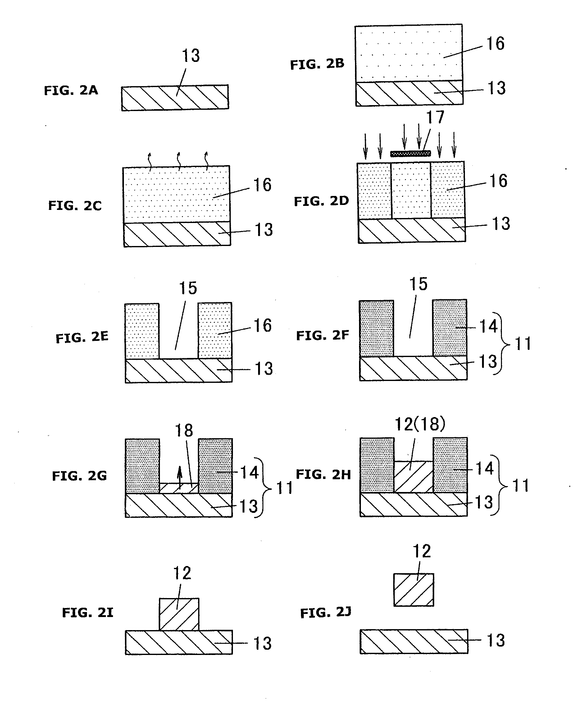
[0061]Next, a process of fabricating the me...

second embodiment

of the Invention

[0094]FIG. 13A is a sectional view of a mold 31 according to a second embodiment of the present invention. In this mold 31, a recess 32 of a desired shape is formed on the upper surface of the conductive base material 13 in the cavity 15, and this recess 32 configures part of the cavity 15. Thus, by electrodepositing a metal inside the cavity 15, the metal-formed product 12 of a more sophisticated shape can be formed.

[0095]Also, while the recess 32 is formed in part of the bottom surface of the cavity 15 in the embodiment depicted in FIG. 13A, the recess 32 may be formed in the entire bottom surface of the cavity 15, as depicted in another embodiment depicted in FIG. 13B.

[0096]Furthermore, in still another embodiment depicted in FIG. 14, the recess 32 is formed on the upper surface of the conductive base material 13 in a range wider than the bottom surface of the cavity 15, and part of the recess 32 is filled with the insulating layer 14.

[0097]Note that when the uppe...

third embodiment

of the Invention

[0098]FIG. 15 is a sectional view of a mold 41 and the metal-formed product 12 along a longitudinal direction according to a third embodiment of the present invention. In the present embodiment, a bottom shape of the cavity 15 in a longitudinal direction is described, by way of example. The description, however, can be applied to a bottom surface in a traverse direction and also to the case where the surfaces in both longitudinal and traverse directions are inclined. However, in any of these cases, electrodeposition in a traverse direction is performed within a range described in the first embodiment. In the present embodiment, in the cross section in the traverse direction, electrodeposition is performed according to the conditions as described in the first embodiment. Furthermore, by performing electroforming also in the longitudinal direction according to the conditions as described in the first embodiment, in comparison between a upper flat part 42a and a lower f...


PUM

PropertyMeasurementUnit
heightaaaaaaaaaa
heightaaaaaaaaaa
heightaaaaaaaaaa

Abstract

A mold is fabricated with a cavity formed in an insulating layer formed so as to be placed on an upper surface of a conductive base material. This mold is disposed in an electrolyte bath to be applied with a voltage, and a metal is electrodeposited on the bottom surface of the cavity to electroform a metal-formed product in the cavity. In this electrodepositing process, when the width of the cavity is taken as W and a vertical height of a head space between an upper opening of the cavity and an upper surface of a metal layer is taken as H, the growth of the metal layer is stopped so that the height H of the head space left above the metal layer satisfies: H≧W/2.85 where 300 μm≦W; H≧W/3.75 where 200 μm≦W<300 μm; H≧W/4 where 100 μm≦W<200 μm; and H≧W/10 where W<100 μm.

Description

BACKGROUND OF INVENTION[0001]1. Technical Field[0002]One or more embodiments of the present invention relate to an electroforming method for molding metal products.[0003]2. Background Art[0004]As a method of manufacturing a fine metal product that is difficult to produce with machining, electroforming technology (electroforming) has been known. This is a thick electroplating process of thickly plating a metal on a mold and removing the thick-plated film (the metal-formed product) from the mold, thereby forming a metal product. In general, electroplating with a thickness exceeding 20 μm is called electroforming.[0005]For example, in a method disclosed in Patent Document 1, the surface of a metal-made mold is coated with a photoresist, and is then patterned to form a resist film with an opening of a desired pattern, and then a metal is electrodeposited inside the opening of the resist film, that is, on a part of the surface of the mold not coated with the resist film to form a metal l...

Claims


Application Information

Patent Timeline
Patent Type & Authority Applications(United States)
IPC IPC(8): C25D1/10
CPCC25D5/022H05K3/205C25D1/20C25D1/10C25D1/003C25D1/00
Inventor SEKI, KAZUMASAHATAMURA, AKIHIKOYOSHIDA, HITOSHIYAMASHITA, TOSHIOMIURA, YASUHIRO
Owner ORMON CORP
Why Eureka
Try Eureka