Lead frame for semiconductor device

Active Publication Date: 2011-10-13
NXP USA INC
View PDF12 Cites 14 Cited by
  • Summary
  • Abstract
  • Description
  • Claims
  • Application Information

AI Technical Summary

Benefits of technology

[0017]An aspect of the invention is a method of forming a lead frame for a semiconductor package, the method comprises providing a lead frame having a die bond area for receiving a semiconductor die and a plurality of leads arranged around and spaced apart from the die bond area for being electrically interconnected with the semiconductor die and for providing electrical interconnection for the semiconductor package device, the leads having a top surface and a bottom surface; removing a portion from the top surface to form a recessed portion of a first lead in the plurality of leads; and removing a portion from the bottom surface to form a recessed portion of a second lead adjacent to the first lead for reducing burr formation effects.

Problems solved by technology

The burr 22 can lead to device failure as the smeared material may cause shorting between adjacent leads.
That is, there is a growing risk of burr formation and shorting.

Method used


Image

  • Lead frame for semiconductor device
  • Lead frame for semiconductor device
  • Lead frame for semiconductor device

Examples


Embodiment Construction

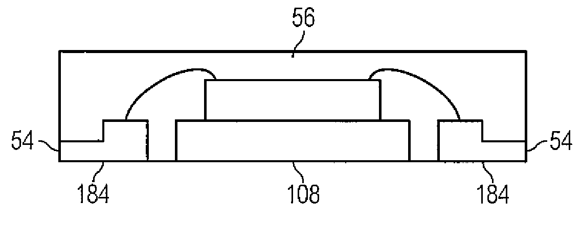
[0012]An aspect of the invention is a lead frame for supporting a semiconductor die within a semiconductor package device, the lead frame comprising a die bond area for receiving a semiconductor die; and a plurality of leads arranged around and spaced apart from the die bond area for being electrically interconnected with the semiconductor die and for providing electrical interconnection for the semiconductor package device, the leads having a top surface and a bottom surface, wherein a first lead in the plurality of leads has a recessed portion from the top surface, and a second lead adjacent to the first lead has a recessed portion from the bottom surface for reducing burr formation effects.

[0013]In an embodiment the plurality of leads are arranged in a single row around the perimeter of the die bond area. The plurality of leads may comprise a plurality of first leads with the recessed portion from the top surface that form a first row, and a plurality of second leads with a reces...


PUM


Abstract

A lead frame for reducing detrimental effects of burr formation includes a lead frame that has leads where a portion of a top surface is removed from a first lead and a portion of a bottom surface is removed from a second lead adjacent to the first lead to reduce spacing between leads while reducing the detrimental effects of burr formation, such as shorting and the like, caused during singulation of a semiconductor device manufactured with the lead frame.

Description

BACKGROUND OF THE INVENTION[0001]The present invention relates generally to semiconductor packaging, and more particularly to a lead frame for packaging semiconductor devices that reduces the detrimental effects of burr formation during the singulation process.[0002]Conventional semiconductor package devices 10, such as single row lead frame design quad flat no-lead (QFN) packages as shown in FIGS. 1A-1B, typically are assembled using matrix array packaging (MAP). MAP type semiconductor package devices are processed and manufactured as multiple semiconductor package devices on a single substrate bar unit. During assembly, the single substrate bar unit is divided into individual and discrete semiconductor package devices by a singulation process.[0003]Each semiconductor package device 10 typically includes a lead frame with leads 12 and die bond area 14. A semiconductor integrated circuit (IC) die (not shown in FIGS. 1A-1B) is fixed or bonded to the die bond area 14 of the lead frame...

Claims


Application Information

Patent Timeline
IPC IPC(8): H01L23/495H01L21/60
CPCH01L23/3107H01L24/48H01L24/29H01L24/32H01L24/45H01L24/83H01L24/85H01L24/97H01L2224/32245H01L2224/45144H01L2224/48091H01L2224/48247H01L2224/73265H01L2224/92247H01L2224/97H01L2924/01029H01L2924/01033H01L2924/01046H01L2924/0105H01L2924/01078H01L2924/01079H01L2924/01082H01L2924/014H01L2924/0665H01L23/49548H01L2924/01005H01L2924/01006H01L2224/85H01L2924/01028H01L2224/83H01L2924/15747H01L2924/00014H01L2924/00H01L2924/181H01L2924/14H01L2924/00012
Inventor LU, YONGSHENGTIAN, BINXU, NANYAO, JINZHONGZHAO, SHUFENG
Owner NXP USA INC
Why Eureka
Try Eureka