

Resonator element, resonator, and piezoelectric device
- Summary
- Abstract
- Description
- Claims
- Application Information
AI Technical Summary
Benefits of technology
Problems solved by technology
Method used
Image

Examples
first embodiment
[0046]First, a first embodiment of the invention will be described.
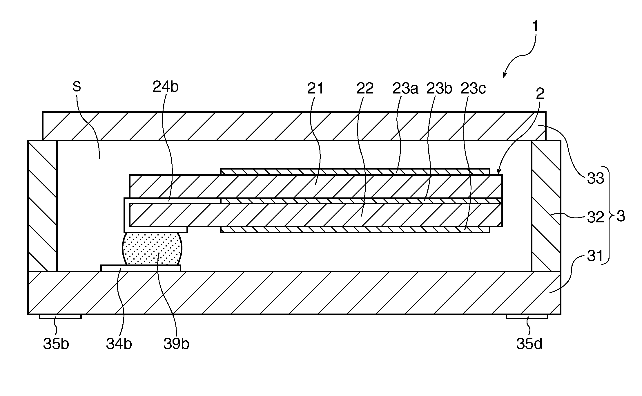
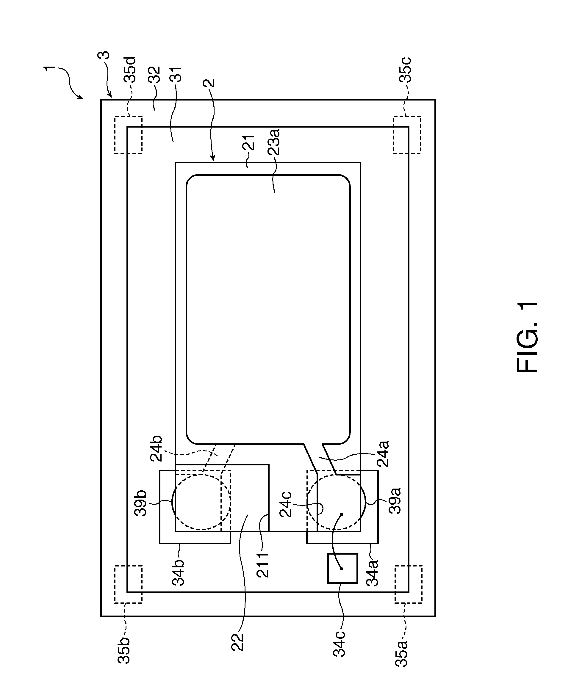
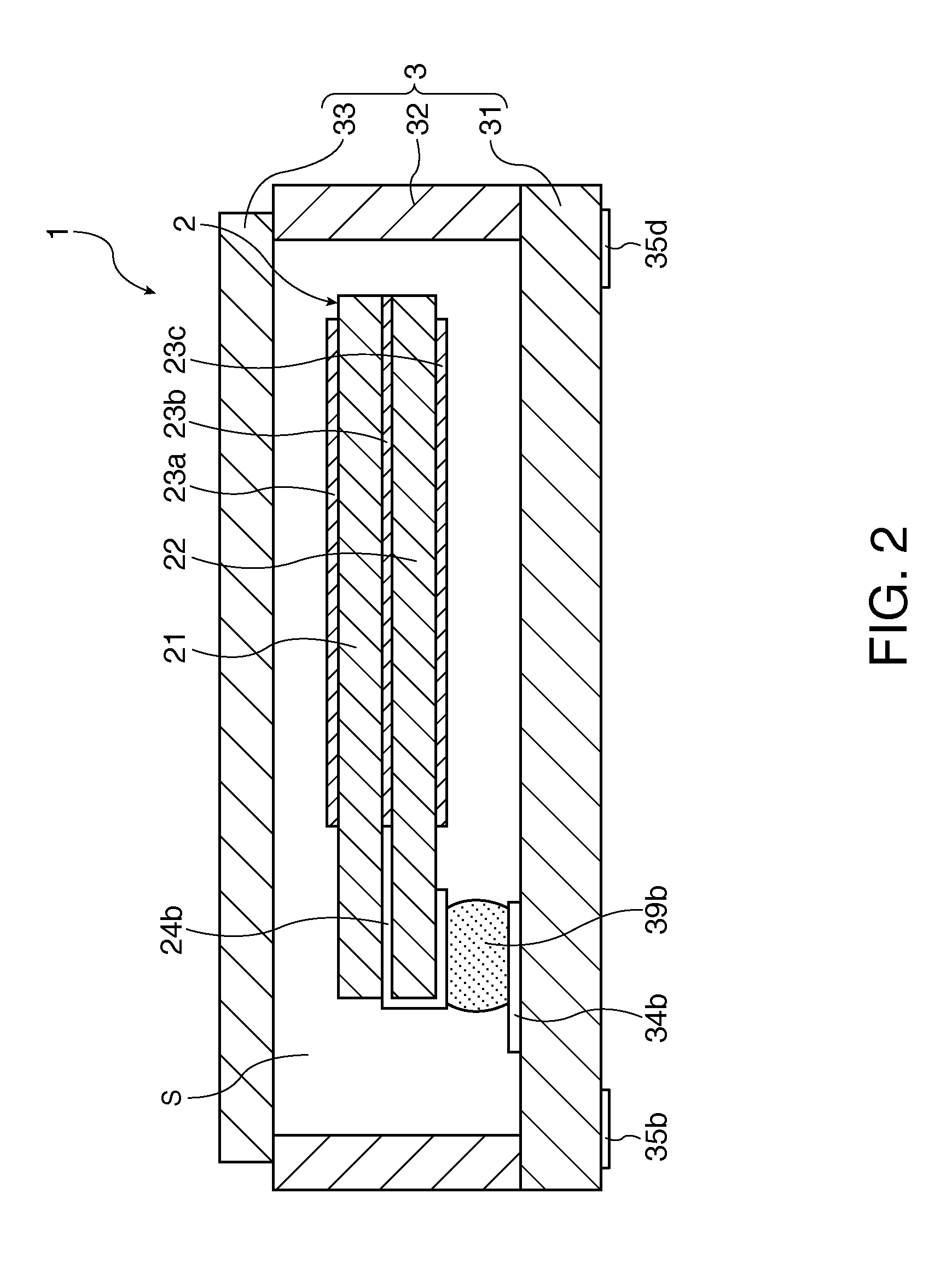
[0047]FIG. 1 is a top view illustrating a piezoelectric device (resonator) according to the first embodiment of the invention. FIG. 2 is a cross-sectional view of the piezoelectric device illustrated in FIG. 1. FIG. 3 is a schematic diagram for explaining an operation of a resonator element included in the piezoelectric device illustrated in FIG. 2. FIG. 4 is a diagram for explaining a first example of a case where a first piezoelectric substrate and a second piezoelectric substrate included in the resonator element illustrated in FIG. 3 are made of AT-cut quartz crystals. FIG. 5 is a diagram for explaining a second example of the case where the first piezoelectric substrate and the second piezoelectric substrate included in the resonator element illustrated in FIG. 3 are made of AT-cut quartz crystals. In addition, in the following description, for the convenience of description, the upper side in FIG. 2 is referred...
second embodiment
[0089]Next, a piezoelectric device according to a second embodiment of the invention will be described.
[0090]FIG. 6 is a cross-sectional view of a resonator element included in the piezoelectric device according to the second embodiment of the invention.
[0091]Hereinafter, differences between the piezoelectric device according to the second embodiment and that according to the above embodiment are mainly described, and description of the same configurations will be omitted.
[0092]The piezoelectric device according to the second embodiment is substantially the same as that according to the first embodiment except that the formation range of an electrode layer between first and second piezoelectric substrates is different. In addition, in FIG. 6, illustration of connection electrodes is omitted. In addition, like elements as described in the above embodiment are denoted by like reference numerals.
[0093]In a resonator element 2A of the piezoelectric device according to this embodiment, a...
third embodiment
[0097]Next, a piezoelectric device according to a third embodiment of the invention will be described.
[0098]FIG. 7 is a cross-sectional view of a resonator element included in the piezoelectric device according to the third embodiment of the invention.
[0099]Hereinafter, differences between the piezoelectric device according to the third embodiment and those according to the above embodiments are mainly described, and description of the same configurations will be omitted.
[0100]The piezoelectric device according to the third embodiment is substantially the same as that according to the first embodiment except that the formation range of an electrode layer between first and second piezoelectric substrates is different and the resonator element has a mesa structure. In addition, the piezoelectric device according to the third embodiment is substantially the same as that according to the second embodiment except that the resonator element has the mesa structure. In addition, in FIG. 7, ...
PUM
 Abstract
Description
Claims
Application Information