Wafer-Bump Structure
a wafer-bump and structure technology, applied in the direction of electrical equipment, semiconductor devices, semiconductor/solid-state device details, etc., can solve the problems of low yield high cost of the conventional under-bump metallization process, etc., to achieve the effect of inexpensive wafer-bump structur
- Summary
- Abstract
- Description
- Claims
- Application Information
AI Technical Summary
Benefits of technology
Problems solved by technology
Method used
Image

Examples
Embodiment Construction
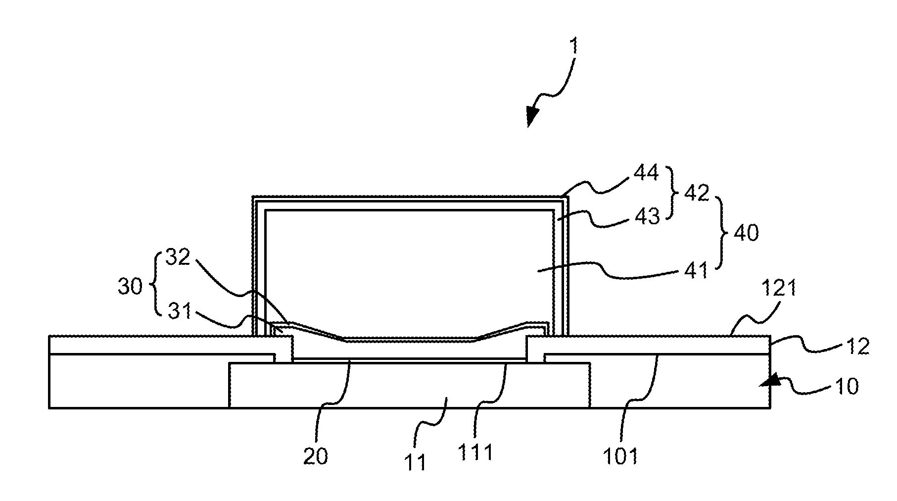
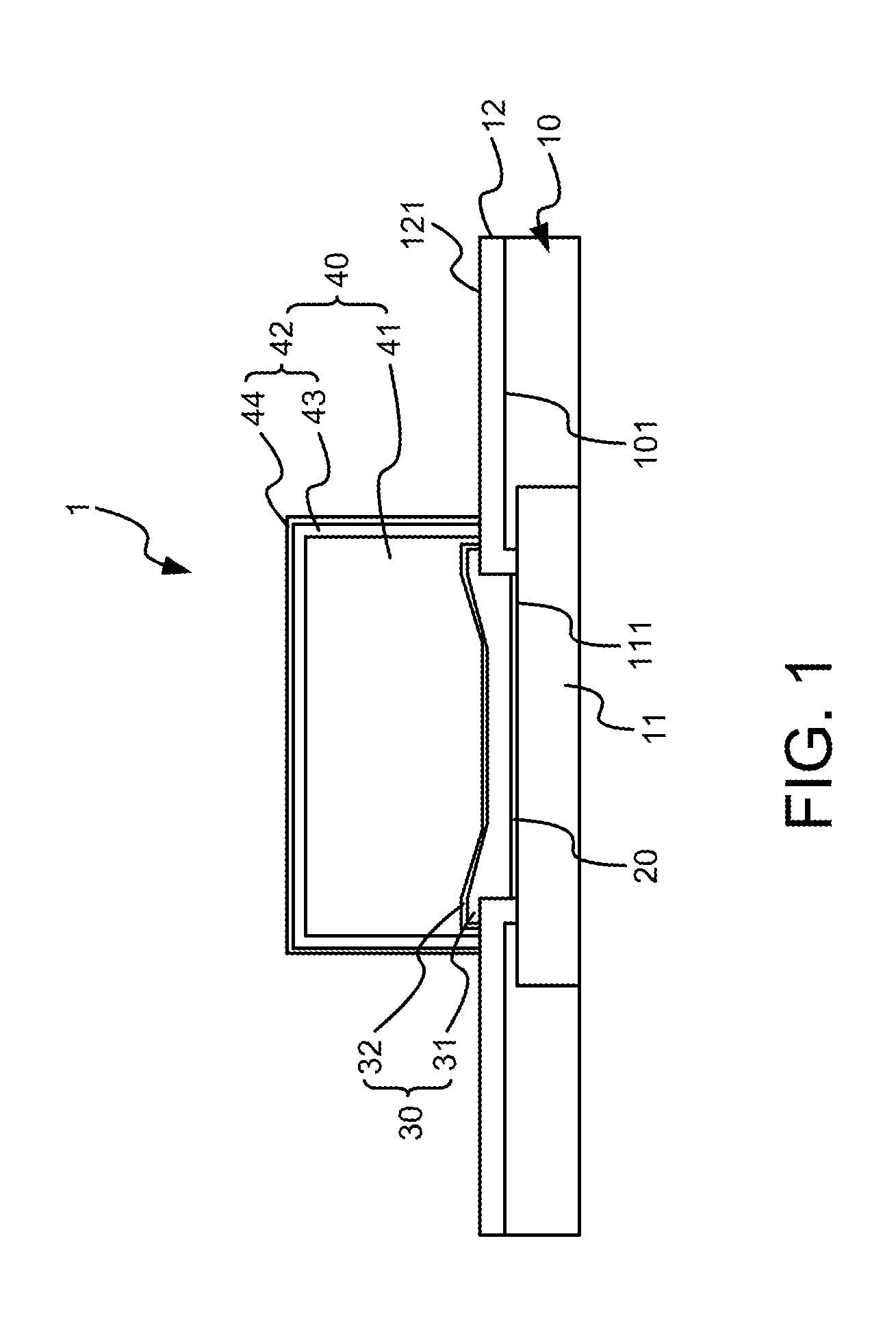
[0013]Referring to FIG. 1, there is shown a wafer-bump structure 1 according to the preferred embodiment of the present invention. The wafer-bump structure 1 includes a wafer-state semiconductor die 10, a pre-treatment layer 20, a first electrodeless nickel / immersion gold laminate 30 and at least one pillar bump 40.
[0014]The wafer-state semiconductor die 10 is formed with a surface 101. At least one die pad 11 is embedded in the semiconductor die 10. A passivation layer 12 is formed on the surface 101 of the semiconductor die 10 and a surface 111 of the die pad 11. The passivation layer 12 includes at least one aperture for allowing access to a portion of the surface 111 of the die pad 11.
[0015]The pre-treatment layer 20 is formed on the portion of the surface 111 of the die pad 11 that is not covered by the aperture defined in the passivation layer 12. The pre-treatment layer 20 is an anti-erosion layer made in a zincating process.
[0016]The first electrodeless nickel / immersion gold...
PUM
 Abstract
Description
Claims
Application Information
 - Generate Ideas
- Intellectual Property
- Life Sciences
- Materials
- Tech Scout
- Unparalleled Data Quality
- Higher Quality Content
- 60% Fewer Hallucinations
Browse by: Latest US Patents, China's latest patents, Technical Efficacy Thesaurus, Application Domain, Technology Topic, Popular Technical Reports.
© 2025 PatSnap. All rights reserved.Legal|Privacy policy|Modern Slavery Act Transparency Statement|Sitemap|About US| Contact US: help@patsnap.com