Structure and method for air gap interconnect integration

a technology of metal insulation and interconnect structure, which is applied in the field of air gap-containing metal insulation interconnect structure, can solve the problems of affecting the propagation of information, affecting the quality of etc., to achieve cheap and reliable air gap-containing interconnect structure, high resolution, and increase the cost of air gap module

Active Publication Date: 2011-11-10
ALSEPHINA INNOVATIONS INC
View PDF4 Cites 19 Cited by
  • Summary
  • Abstract
  • Description
  • Claims
  • Application Information

AI Technical Summary

Benefits of technology

[0006]Finally, the need for very high resolution lithography and a critical etch step leads to a huge increase in the cost of the air gap module. Thus, there is a need for a simplified integration scheme that leads to cheap and reliable air gap-containing interconnect structures.

Problems solved by technology

Interconnect structures in integrated circuits induce a delay in the propagation of the information between semiconductor devices such as transistors.
There are several problems with the aforementioned prior art air gap fabrication scheme.
If the lithography step is not perfect (misalignment, or too large an opening may result) and, if the etch step leads to a width increase, the metal lines can be damaged by this etch step.
The isotropic etch process may also damage the sidewalls of the metal line or the interface between the metal lines and an overlying cap layer.
Both issues may lead to reliability issues.

Method used


Image

  • Structure and method for air gap interconnect integration
  • Structure and method for air gap interconnect integration
  • Structure and method for air gap interconnect integration

Examples


Embodiment Construction

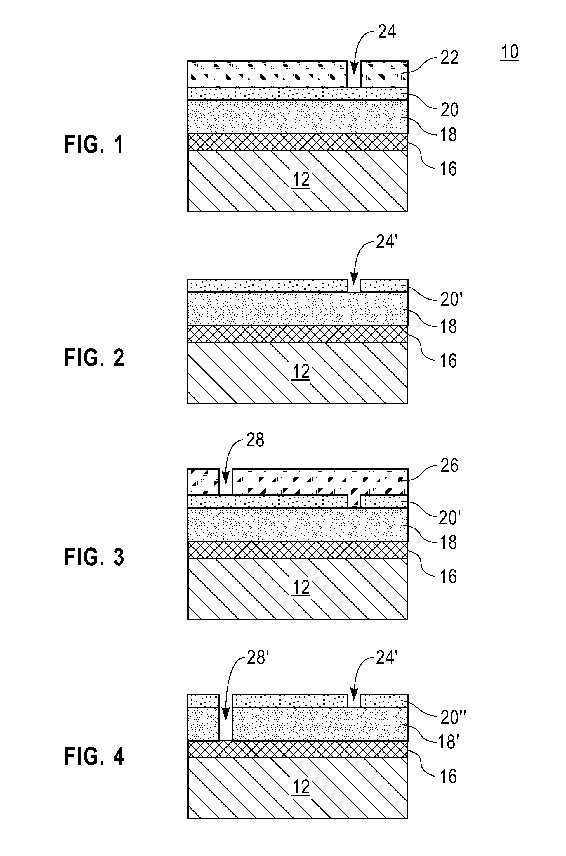
ching exposed portions of the first low k material and removal of the patterned photoresist.

[0023]FIG. 12 is a pictorial representation (through a cross sectional view) depicting the structure of FIG. 11 after forming a patterned and cured photo-patternable low k material having a plurality of electrically conductive filled regions and gaps located therein, wherein at least one of the plurality of electrically conductive filled regions is located within an opening that is present in the previously etched portions of the first low k material.

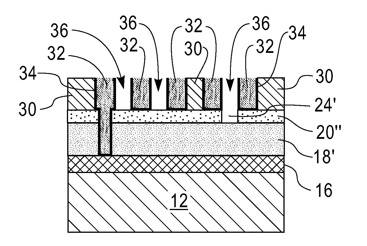
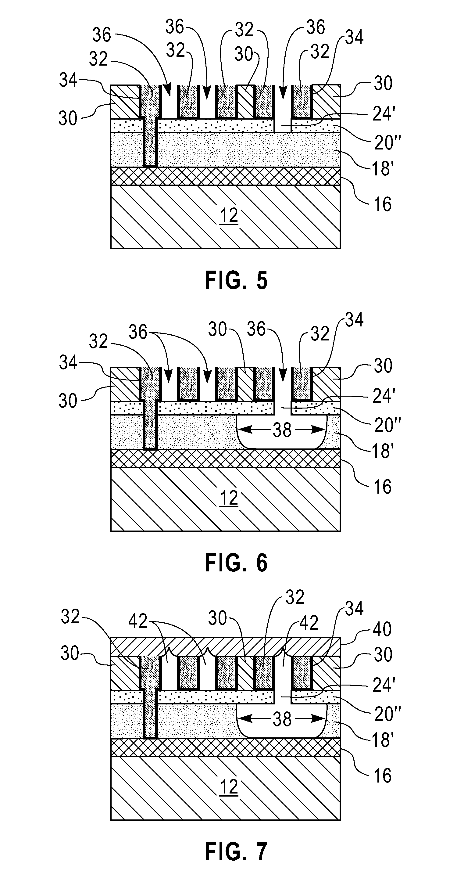
[0024]FIG. 13 is a pictorial representation (through a cross sectional view) depicting the structure of FIG. 12 after performing a lateral etch that expands the width of at least one of the gaps.

[0025]FIG. 14 is a pictorial representation (through a cross sectional view) depicting the structure of FIG. 13 after forming a dielectric cap atop the patterned and cured photo-patternable low k material forming air gaps within the structure.

DETAILED DES...


PUM

PropertyMeasurementUnit
widthaaaaaaaaaa
dielectric constantaaaaaaaaaa
temperatureaaaaaaaaaa

Abstract

Methods for producing air gap-containing metal-insulator interconnect structures for VLSI and ULSI devices using a photo-patternable low k material as well as the air gap-containing interconnect structure that is formed are disclosed. More particularly, the methods described herein provide interconnect structures built in a photo-patternable low k material in which air gaps are defined by photolithography in the photo-patternable low k material. In the methods of the present invention, no etch step is required to form the air gaps. Since no etch step is required in forming the air gaps within the photo-patternable low k material, the methods disclosed in this invention provide highly reliable interconnect structures.

Description

RELATED APPLICATIONS[0001]This application is related to co-pending and co-assigned U.S. application Ser. No. 12 / 721,032, entitled “METHODS FOR FABRICATION OF AN AIR GAP-CONTAINING INTERCONNECT STRUCTURE” filed Mar. 10, 2010, and co-pending and co-assigned U.S. application Ser. No. 12 / 768,267, entitled “STRUCTURES AND METHODS FOR AIR GAP INTEGRATION” filed Apr. 27, 2010, the entire contents of which are both incorporated herein by reference.FIELD OF THE INVENTION[0002]The present invention relates to air gap-containing metal-insulator interconnect structures for Very Large Scale Integrated (VLSI) and Ultra-Large Scale Integrated (ULSI) devices and methods of forming the same.BACKGROUND OF THE INVENTION[0003]Interconnect structures in integrated circuits induce a delay in the propagation of the information between semiconductor devices such as transistors. To reduce this delay, the interconnect structures should posses the lowest capacitance possible. One approach to form interconnec...

Claims


Application Information

Patent Timeline
Patent Type & Authority Applications(United States)
IPC IPC(8): H01L23/522G03F7/20
CPCH01L21/02126H01L2924/12044H01L21/02282H01L21/02318H01L21/31H01L21/3105H01L21/76807H01L21/7682H01L21/76825H01L21/76826H01L21/76828H01L21/76829H01L21/76835H01L23/5222H01L23/53295H01L2221/1031H01L2221/1036H01L21/02274H01L2924/0002
Inventor CLEVENGER, LAWRENCE A.DARNON, MAXIMELIN, QINGHUANGLISI, ANTHONY D.NITTA, SATYANARAYANA V.
Owner ALSEPHINA INNOVATIONS INC
Why Eureka
Try Eureka