System for concurrent test of semiconductor devices

a test system and semiconductor technology, applied in semiconductor/solid-state device testing/measurement, testing circuits, instruments, etc., can solve the problems of increased complexity of test systems required to test the devices, increased test cost, and increased time requirements

Active Publication Date: 2011-11-10
TERADYNE
View PDF2 Cites 46 Cited by
  • Summary
  • Abstract
  • Description
  • Claims
  • Application Information

AI Technical Summary

Benefits of technology

[0014]In a further aspect, the invention relates to a method of operating a computing device to generate information for a plan for concurrent test of at least one device, each of the at least one devices having a plurality of pins, and the test being performed by a test system having a plurality of resources connectable to the plurality of pins, the concurrent test comprising a plurality of blocks. The method includes iteratively performing processing that includes identifying a candidate flow in accordance with a heuristic, the candidate flow scheduling blocks to avoid previously identified conflicts between blocks. For each candidate flow, an attempt is made to allocate resources of the plurality of resources to pins of the plurality of pins to execute the concurrent test according to the candidate flow. When the attempt to allocate results in a successful allocation of resources, the test time for executing the concurrent test using the candidate flow is computed. When an allocation of resources is not successful because of a conflict between test blocks, the conflict between conflicting test blocks is recorded so that candidate flows in subsequent iterations do not include the conflict.
[0015]In yet a further aspect, the invention relates to at least one computer-readable storage medium comprising a plurality of computer-executable instructions that, when executed by at least one processor, implement a tool for generating information for a plan for concurrent test of at least one device, each of the at least one devices having a plurality of pins, and the test being performed by a test system having a plurality of resources connectable to the plurality of pins, the concurrent test comprising a plurality of blocks. The computer-executable instructions make up a plurality of modules, plurality of modules comprising at least two modules, which may be two or more modules. A first possible module may, in response to input designating a first technique, identify at least one flow for concurrent test by enumerating candidate flows; attemp...

Problems solved by technology

As devices have gotten more complex, the complexity of test systems required to test the devices has increased.
Additionally, more time is required to create test plans and to perform the tests, creating a concern for device manufacturers over the cost of test.
Accordingly, a difficulty in making a concurrent test plan is identifying an appropriate test “flow” in which all test blocks are eventually executed, but that includes appropriate test blocks being executed together to save more test time.
A further difficulty in making a current test p...

Method used


Image

  • System for concurrent test of semiconductor devices
  • System for concurrent test of semiconductor devices
  • System for concurrent test of semiconductor devices

Examples


Embodiment Construction

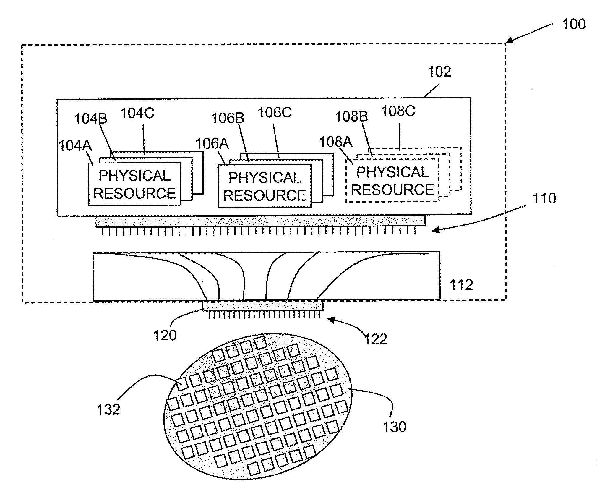
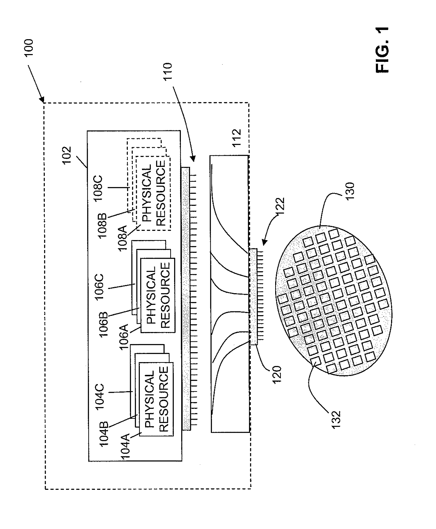
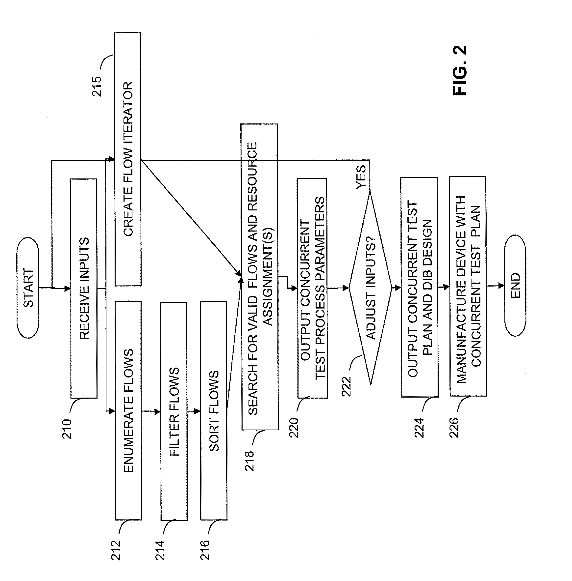
[0034]The inventors have recognized and appreciated that an automated tool for mapping tester channels to pins can speed development of a concurrent test plan and may yield a more cost effective concurrent test plan. By having a tool that can quickly make an efficient assignment, values of multiple parameters in the concurrent test plan can be varied to search for a plan that makes appropriate tradeoffs between test time and test equipment costs. Use of the tool may lead to identification of a test system configuration, test flow and channel assignments that provide a desired tradeoff between time and cost for testing a particular device.

[0035]Such a tool may address challenges associated with identifying concurrent flows that can be achieved for particular testing scenarios. The tool, for example, may aid a user in identifying device-enabled flows by identifying blocks that are fully independent from each other or, conversely, conflicting blocks that cannot be tested concurrently. ...


PUM


Abstract

A tool to aid a test engineer in creating a concurrent test plan. The tool may quickly map test system resources to specific pins to satisfy the requirements of a concurrent test. The tool may project test time when such a mapping is possible. When a mapping is not possible, the tool may inform its user, including making suggestions of additional resources that could allow the test system to perform the test or suggestions for other variations in input parameters that would allow a mapping. The tool employs an assignment process in which groups of associated pins are identified, along with associated resource requirements for each group. Groups of test system resources that collectively fulfill a higher level requirement are identified and the assignment is made by mapping resource sets to resource groups, using ordering and matching heuristics to reduce processing time.

Description

BACKGROUND[0001]1. Field of the Invention[0002]This invention relates generally to the manufacture of semiconductor devices and more specifically to developing test programs for semiconductor devices.[0003]2. Related Art[0004]Semiconductor devices are generally tested at least once during their manufacture. Such tests are performed by an automated test system that can generate large numbers of stimulus signals and measure large numbers of response signals. The test system has multiple instruments that can generate various types of signals that may occur within a device under test as it operates. Similarly, the instruments can measure the various types of signals that may be generated by the device.[0005]For example, many semiconductor devices are fabricated today as a “system on a chip” (SoC) or a “system in a package” (SiP) that contain sub-circuits, sometimes called “cores” or “functional blocks,” that collectively perform multiple types of operation that may be performed by an el...

Claims


Application Information

Patent Timeline
IPC IPC(8): G06F19/00H01L21/66
CPCG01R31/31907H01L22/20H01L2924/0002H01L2924/00G06F11/263G06F11/22
Inventor VAN WAGENEN, BETHANYEDWARD, SENG J.
Owner TERADYNE
Why Eureka
Try Eureka