Column structure thin film material using metal oxide bearing semiconductor material for solar cell devices

a technology of solar cell devices and thin film materials, applied in the field of photovoltaic materials, can solve the problems of reducing the processing efficiency of solar cell devices, so as to improve processing efficiency, facilitate use, and improve the effect of conversion efficiency

Inactive Publication Date: 2011-11-17
CM MFG
View PDF5 Cites 31 Cited by
  • Summary
  • Abstract
  • Description
  • Claims
  • Application Information

AI Technical Summary

Benefits of technology

[0007]According to embodiments of the present invention, techniques directed to fabrication of photovoltaic cell is provided. More particularly, embodiments according to the present invention provide a method and a structure for a thin film semiconductor material using a metal oxide bearing species. But it would be recognize that embodiments according to the present invention have a much broader range of applicability.
[0010]Depending upon the embodiment, the present invention provides an easy to use process that relies upon conventional technology that can be nanotechnology based. Such nanotechnology based materials and process lead to higher conversion efficiencies and improved processing according to a specific embodiment. In some embodiments, the method may provide higher efficiencies in converting sunlight into electrical power. Depending upon the embodiment, the efficiency can be about 10 percent or 20 percent or greater for the resulting solar cell according to the present invention. Additionally, the method provides a process that is compatible with conventional process technology without substantial modifications to conventional equipment and processes. In a specific embodiment, the present method and structure can also be provided using large scale manufacturing techniques, which reduce costs associated with the manufacture of the photovoltaic devices. In another specific embodiment, the present method and structure can also be provided using solution based processing. In a specific embodiment, the present method uses processes and provides material that are safe to the environment. Depending upon the embodiment, one or more of these benefits may be achieved. These and other benefits will be described in more throughout the present specification and more particularly below.

Problems solved by technology

Unfortunately, petrochemical energy is limited and essentially fixed based upon the amount available on the planet Earth.
Additionally, as more human beings begin to drive and use petrochemicals, it is becoming a rather scarce resource, which will eventually run out over time.
Although solar energy is clean and has been successful to a point, there are still many limitations before it becomes widely used throughout the world.
Crystalline materials are often costly and difficult to make on a wide scale.
Additionally, devices made from such crystalline materials have low energy conversion efficiencies.
Similar limitations exist with the use of thin film technology in making solar cells.
That is, efficiencies are often poor.
Additionally, film reliability is often poor and cannot be used for extensive periods of time in conventional environmental applications.

Method used


Image

  • Column structure thin film material using metal oxide bearing semiconductor material for solar cell devices
  • Column structure thin film material using metal oxide bearing semiconductor material for solar cell devices
  • Column structure thin film material using metal oxide bearing semiconductor material for solar cell devices

Examples


Embodiment Construction

[0015]According to embodiments of the present invention, techniques for forming a thin film metal oxide semiconductor material are provided. More particularly, embodiments according to the present invention provide a method and structures for thin film metal oxide semiconductor material for solar cell application. But it would be recognized that embodiments according to the present invention have a much broader range of applicability.

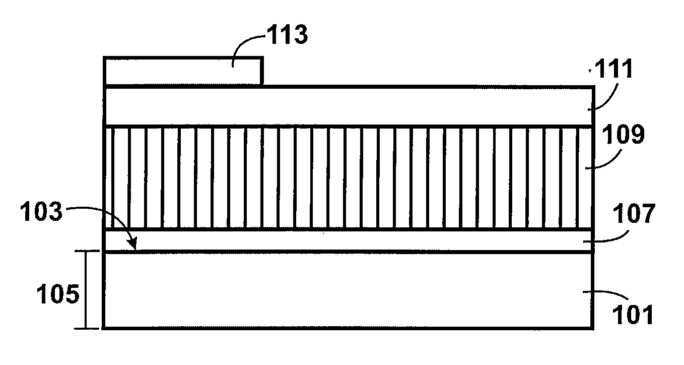
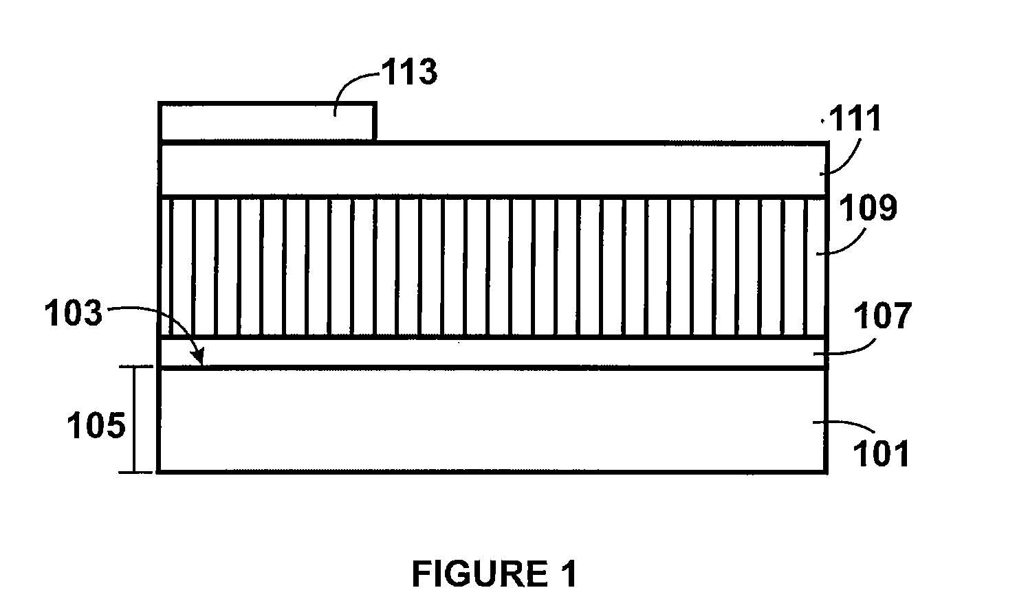
[0016]FIG. 1 is a simplified diagram illustrating a solar cell device structure using a thin metal oxide semiconductor film structure for solar cell application according to an embodiment of the present invention. The diagram is merely an illustration and should not unduly limit the claims herein. One skilled in the art would recognize other modifications, variations, and alternatives. As shown in FIG. 1, a substrate 101 is provided. The substrate includes a surface region 103 and a thickness 105. The substrate can be a semiconductor such as silicon, si...


PUM


Abstract

A thin film material structure for solar cell devices. The thin film material structure includes a thickness of material comprises a plurality of single crystal structures. In a specific embodiment, each of the single crystal structure is configured in a column like shape. The column like shape has a dimension of about 0.01 micron to about 10 microns characterizes a first end and a second end. An optical absorption coefficient of greater than 104 cm−1 for light in a wavelength range comprising about 400 cm−1 to about 700 cm−1 characterizes the thickness of material.

Description

CROSS-REFERENCES TO RELATED APPLICATIONS[0001]This application is a division of U.S. patent application Ser. No. 12 / 237,371; filed on Sep. 24, 2008, which claims priority to U.S. Provisional Patent Application No. 60 / 976,392; filed on Sep. 28, 2007; the disclosures of both the applications are incorporated by reference herein in their entirety for all purposes.BACKGROUND OF THE INVENTION[0002]The present invention relates generally to photovoltaic materials. More particularly, the present invention provides a method and structure for manufacture of photovoltaic materials using a thin film process including metal oxide bearing materials such as copper oxide and the like. Merely by way of example, the present method and structure have been implemented using a nanostructure configuration, but it would be recognized that the other configurations such as bulk materials may be used.[0003]From the beginning of time, human beings have been challenged to find way of harnessing energy. Energy...

Claims


Application Information

Patent Timeline
Patent Type & Authority Applications(United States)
IPC IPC(8): H01L31/036H01L31/0224
CPCH01L31/0336H01L31/03365H01L31/0352H01L31/0248H01L31/0392Y02E10/50H01L31/03529
Inventor LEE, HOWARD W.H.
Owner CM MFG
Why Eureka
Try Eureka